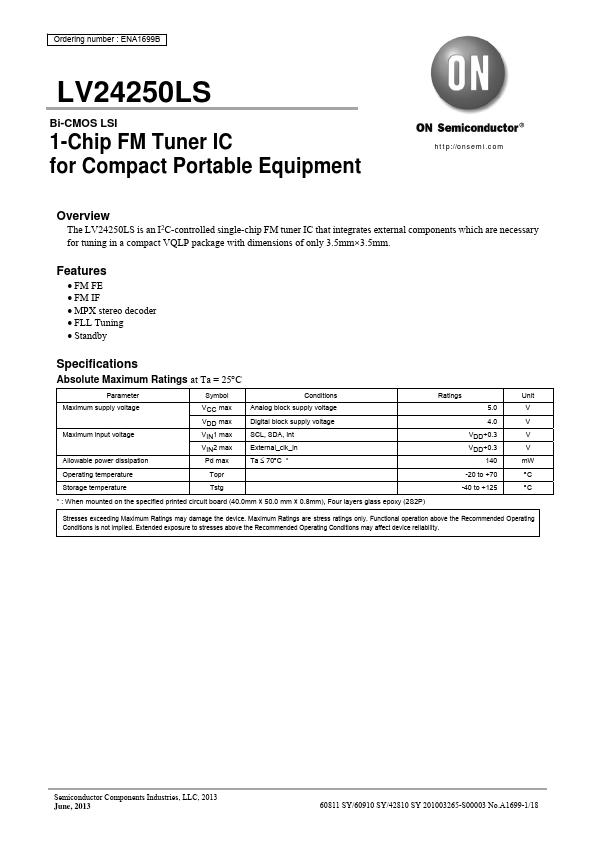
| Part | LV24250LS |
|---|---|
| Description | 1-Chip FM Tuner |
| Manufacturer | onsemi |
| Size | 243.10 KB |
Related Datasheets
| Part Number | Manufacturer | Description |
|---|---|---|
| R820T2 | Rafael Microelectronics | High Performance Low Power Advanced Digital TV Silicon Tuner |
| LA1260 | SANYO | FM/AM Tuner System |
| TDA18275 | NXP Semiconductors | Hybrid (analog and digital) silicon tuner |


