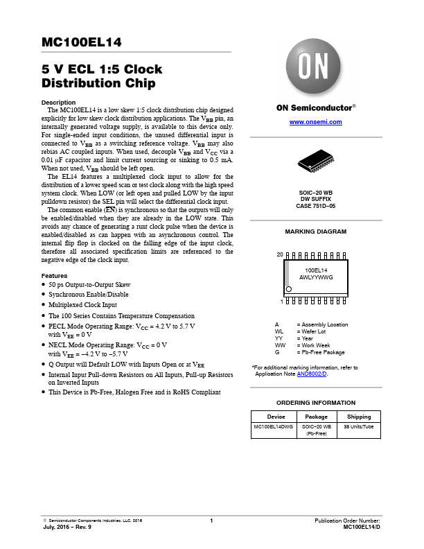
Datasheet4U Logo Datasheet4U.com

MC100EL14 - 1:5 Clock Distribution Chip

General Description

explicitly for low skew clock distribution applications.

The VBB pin, an internally generated voltage supply, is available to this device only.

Key Features

  • a multiplexed clock input to allow for the distribution of a lower speed scan or test clock along with the high speed system clock. When LOW (or left open and pulled LOW by the input pulldown resistor) the SEL pin will select the differential clock input. The common enable (EN) is synchronous so that the outputs will only be enabled/disabled when they are already in the LOW state. This avoids any chance of generating a runt clock pulse when the device is enabled/disabled as can happen with an as.

📥 Download Datasheet

Datasheet Details

Part number MC100EL14
Manufacturer onsemi
File Size 137.41 KB
Description 1:5 Clock Distribution Chip
Datasheet download datasheet MC100EL14 Datasheet

Full PDF Text Transcription (Reference)

The following content is an automatically extracted verbatim text from the original manufacturer datasheet and is provided for reference purposes only.

View original datasheet text
MC100EL14 5 V ECL 1:5 Clock Distribution Chip Description The MC100EL14 is a low skew 1:5 clock distribution chip designed explicitly for low skew clock distribution applications. The VBB pin, an internally generated voltage supply, is available to this device only. For single-ended input conditions, the unused differential input is connected to VBB as a switching reference voltage. VBB may also rebias AC coupled inputs. When used, decouple VBB and VCC via a 0.01 mF capacitor and limit current sourcing or sinking to 0.5 mA. When not used, VBB should be left open. The EL14 features a multiplexed clock input to allow for the distribution of a lower speed scan or test clock along with the high speed system clock.