MC10111
Dual 3- Input/3- Ouput NOR Gate
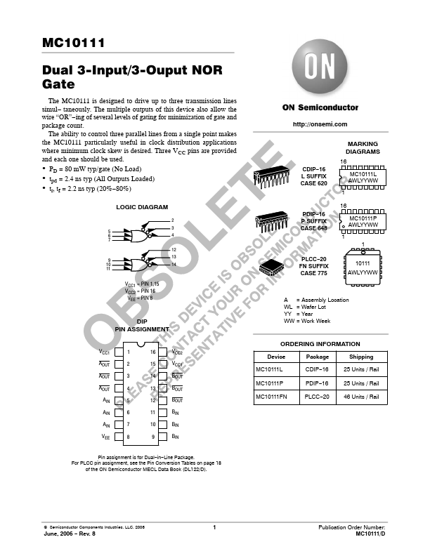
The MC10111 is designed to drive up to three transmission lines simul- taneously. The multiple outputs of this device also allow the wire “OR”- ing of several levels of gating for minimization of gate and package count.
The ability to control three parallel lines from a single point makes the MC10111 particularly useful in clock distribution applications where minimum clock skew is desired. Three VCC pins are provided and each one should be used.
- PD = 80 m W typ/gate (No Load)
- tpd = 2.4 ns typ (All Outputs Loaded)
- tr, tf = 2.2 ns typ (20%- 80%)
LOGIC DIAGRAM
2 53 64 7
12 9 13 10 14 11
VCC1 = PIN 1,15 VCC2 = PIN 16 VEE = PIN 8
DIP PIN ASSIGNMENT
VCC1 AOUT AOUT AOUT
AIN AIN AIN VEE
1 2 3 4 5 6 7 8
16 VCC2 15 VCC1 14 BOUT 13 BOUT 12 BOUT 11 BIN 10 BIN 9 BIN
Pin assignment is for Dual- in- Line Package. For PLCC pin assignment, see the Pin Conversion Tables on page 18 of the ON Semiconductor MECL Data Book (DL122/D). http://onsemi.
CDIP- 16 L...