MC10H117
MC10H117 is Dual 2-Wide 2-3-Input OR-AND/OR-AND Gate manufactured by onsemi.
Description
T h e M C 1 0 H 11 7 d u a l 2
- w i d e 2
- 3
- i n p u t O R
- A N D / OR- AND- Invert gate is a general purpose logic element designed for use in data control, such as digital multiplexing or data distribution. Pin 9 is mon to both gates. This MECL 10H™ part is a functional/pinout duplication of the standard MECL 10K™ family part, with 100% improvement in propagation delay, and no increase in power- supply current.
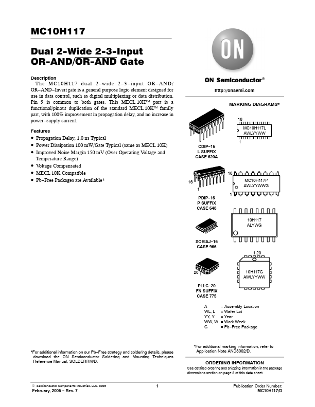
Features http://onsemi. MARKING DIAGRAMS-
16 MC10H117L AWLYYWW CDIP- 16 L SUFFIX CASE 620A 1
- Propagation Delay, 1.0 ns Typical
- Power Dissipation 100 m W/Gate Typical (same as MECL 10K)
- Improved Noise Margin 150 m V (Over Operating Voltage and
- Voltage pensated
- MECL 10K patible
- Pb- Free Packages are Available-
Temperature Range)
16 16 1 PDIP- 16 P SUFFIX CASE 648 1 MC10H117P AWLYYWWG
10H117 ALYWG
SOEIAJ- 16 CASE 966 1 20
20 1 PLLC- 20 FN SUFFIX CASE 775 A WL, L YY, Y WW, W G
10H117G AWLYYWW
= Assembly Location = Wafer Lot = Year = Work Week = Pb- Free Package
- For additional information on our Pb- Free strategy and soldering details, please download the ON Semiconductor Soldering and Mounting Techniques Reference Manual, SOLDERRM/D.
- For additional marking information, refer to Application Note AND8002/D.
ORDERING INFORMATION
See detailed ordering and shipping information in the package dimensions section on page 3 of this data sheet.
© Semiconductor ponents Industries, LLC, 2006
February, 2006
- Rev. 7
Publication Order Number: MC10H117/D
4 5 6 7 9 10 11 12 13 VCC1 = PIN 1 VCC2 = PIN 16 VEE = PIN 8 14 15 3 2 VCC1 AOUT AOUT A1IN A1IN A2IN A2IN VEE 1 2 3 4 5 6 7 8 16 15 14 13 12 11 10 9 VCC2 BOUT BOUT B1IN B1IN B2IN B2IN A2IN, B2IN
Pin assignment is for Dual- in- Line Package.
Figure 1. Logic Diagram
Figure 2. Pin Assignment
Table 1. MAXIMUM RATINGS
Symbol VEE VI Iout TA Tstg Power Supply (VCC = 0) Input Voltage (VCC = 0) Output Current Continuous Surge Characteristic Rating
- 8.0 to 0 0 to VEE 50 100 0 to +75...