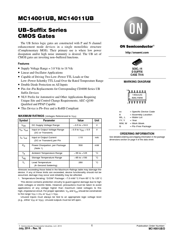
MC14011UB Datasheet Text
MC14001UB, MC14011UB
UB-Suffix Series CMOS Gates
The UB Series logic gates are constructed with P and N channel enhancement mode devices in a single monolithic structure (plementary MOS). Their primary use is where low power dissipation and/or high noise immunity is desired. The UB set of CMOS gates are inverting non- buffered functions.
Features
- Supply Voltage Range = 3.0 Vdc to 18 Vdc
- Linear and Oscillator Applications
- Capable of Driving Two Low- Power TTL Loads or One
Low- Power Schottky TTL Load Over the Rated Temperature Range
- Double Diode Protection on All Inputs
- Pin- for- Pin Replacements for Corresponding CD4000 Series UB
Suffix Devices
- NLV Prefix for Automotive and Other Applications Requiring
Unique Site and Control Change Requirements; AEC- Q100 Qualified and PPAP Capable
- This Device is Pb- Free and is RoHS pliant
MAXIMUM RATINGS (Voltages Referenced to VSS)
Symbol
Parameter
Value
Unit
VDD Vin, Vout
DC Supply Voltage Range
Input or Output Voltage Range (DC or Transient)
- 0.5 to +18.0
- 0.5 to VDD + 0.5
V V
Iin, Iout
Input or Output Current (DC or Transient) per Pin
± 10 mA
PD Power Dissipation, per Package (Note 1)
500 mW...