Datasheet4U Logo Datasheet4U.com

MC14015B - Dual 4-Bit Static Shift Register

Key Features

  • Diode Protection on All Inputs.
  • Supply Voltage Range = 3.0 Vdc to 18 Vdc.
  • Logic Edge.
  • Clocked Flip.
  • Flop Design.
  • Logic State is Retained Indefinitely with Clock Level either High or Low; Information is Transferred to the Output only on the Positive-going Edge of the Clock Pulse.
  • Capable of Driving Two Low.
  • power TTL Loads or One Low.
  • power Schottky TTL Load Over the Rated Temperature Range.
  • NLV Prefix for Automoti.

📥 Download Datasheet

Datasheet Details

Part number MC14015B
Manufacturer onsemi
File Size 166.57 KB
Description Dual 4-Bit Static Shift Register
Datasheet download datasheet MC14015B Datasheet

Full PDF Text Transcription (Reference)

The following content is an automatically extracted verbatim text from the original manufacturer datasheet and is provided for reference purposes only.

View original datasheet text
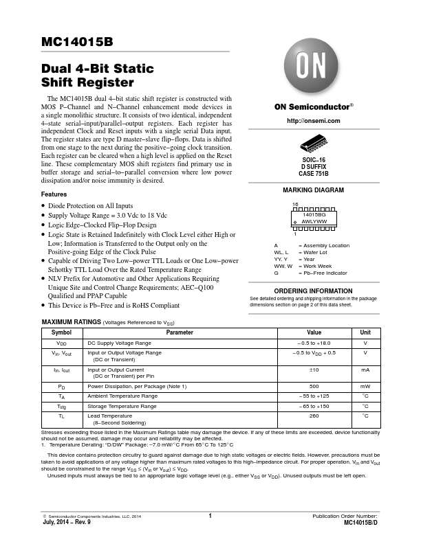
MC14015B Dual 4-Bit Static Shift Register The MC14015B dual 4−bit static shift register is constructed with MOS P−Channel and N−Channel enhancement mode devices in a single monolithic structure. It consists of two identical, independent 4−state serial−input/parallel−output registers. Each register has independent Clock and Reset inputs with a single serial Data input. The register states are type D master−slave flip−flops. Data is shifted from one stage to the next during the positive−going clock transition. Each register can be cleared when a high level is applied on the Reset line. These complementary MOS shift registers find primary use in buffer storage and serial−to−parallel conversion where low power dissipation and/or noise immunity is desired.