MC14050B Description
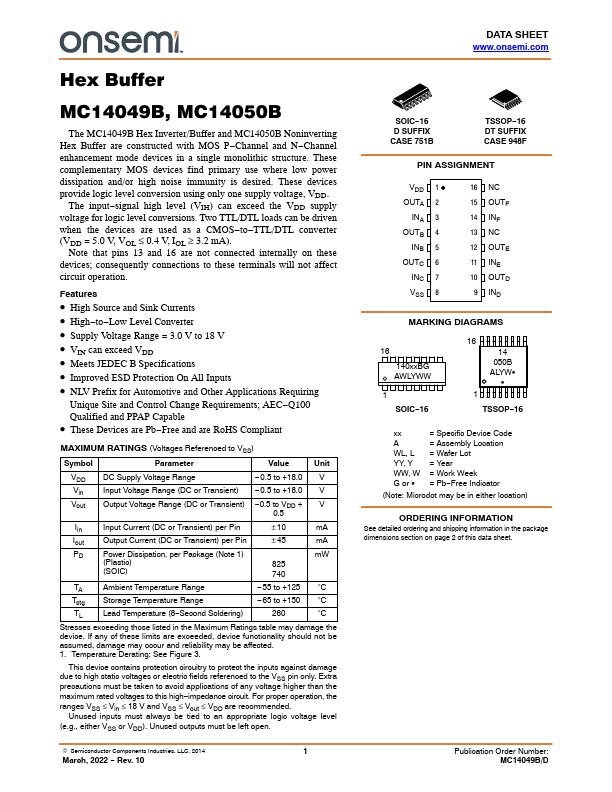
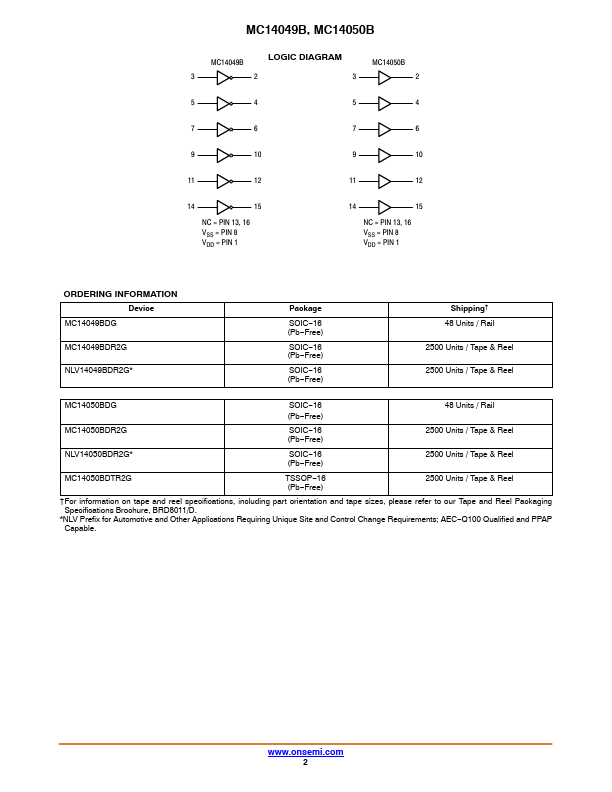
Hex Buffer MC14049B, MC14050B The MC14049B Hex Inverter/Buffer and MC14050B Noninverting Hex Buffer are constructed with MOS P−Channel and N−Channel enhancement mode devices in a single monolithic structure. These plementary MOS devices find primary use where low power dissipation and/or high noise immunity is desired. These devices provide logic level conversion using only one supply voltage, VDD.
MC14050B Key Features
- High Source and Sink Currents
- High-to-Low Level Converter
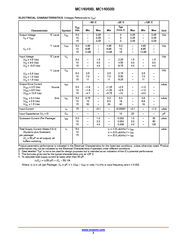
- Supply Voltage Range = 3.0 V to 18 V
- VIN can exceed VDD
- Meets JEDEC B Specifications
- Improved ESD Protection On All Inputs
- NLV Prefix for Automotive and Other