MC14543B
Features
- Latch Storage of Code
- Blanking Input
- Readout Blanking on All Illegal Input binations
- Direct LED (mon Anode or Cathode) Driving Capability
- Supply Voltage Range = 3.0 V to 18 V
- Capable of Driving 2 Low- power TTL Loads, 1 Low- power Schottky
TTL Load or 2 HTL Loads Over the Rated Temperature Range
- Pin- for- Pin Replacement for CD4056A (with Pin 7 Tied to VSS).
- Chip plexity: 207 FETs or 52 Equivalent Gates
- NLV Prefix for Automotive and Other Applications Requiring
Unique Site and Control Change Requirements; AEC- Q100 Qualified and PPAP Capable.
- This Device is Pb- Free and is Ro HS pliant http://onsemi.
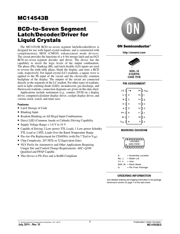
SOIC- 16 D SUFFIX CASE 751B
PIN ASSIGNMENT
LD 1 C2 B3 D4 A5
PH 6 BI 7 VSS 8
16 VDD 15 f 14 g 13 e 12 d 11 c 10 b
9a
MARKING DIAGRAM
16 14543BG AWLYWW
= Assembly Location
WL, L = Wafer Lot
YY, Y = Year
WW, W = Work Week
= Pb- Free Package
ORDERING INFORMATION
See detailed ordering and shipping information in the package dimensions section on page...