MC3479
Features http://onsemi.
- -
- -
- -
- -
- -
Single Supply Operation: 7.2 to 16.5 V 350 m A/Coil Drive Capability Clamp Diodes Provided for Back- EMF Suppression Selectable CW/CCW and Full/Half Step Operation Selectable High/Low Output Impedance (Half Step Mode) TTL/CMOS patible Inputs Input Hysteresis: 400 m V Minimum Phase Logic Can Be Initialized to Phase A Phase A Output Drive State Indication (Open- Collector) Pb- Free Package is Available-
PDIP- 16 P SUFFIX CASE 648C
MARKING DIAGRAM
16 MC3479P AWLYYWWG
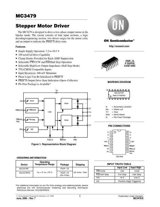
Clk
Clock Driver
..
L1
L2 CW/CCW CW/CCW Logic VD L3 Full/Half Step F/H Step Driver L4 OIC OIC
A WL YY WW G
= Assembly Location = Wafer Lot = Year = Work Week = Pb- Free Package
PIN CONNECTIONS
VD L2 L1 1 2 3 4 5 6 7 8 16 15 14 13 12 11 10 9 VM L3 L4 GND Phase A CW/CCW Full/Half Step
Phase A
Bias/Set
Figure 1. Representative Block Diagram
Bias/Set Clk OIC
ORDERING INFORMATION
Device MC3479P MC3479PG TA = 0° to +70°C Operating Temperature Range Package PDIP-...