MC74ACT00
Features
- Output Drive Capability: $24 m A
- Operating Voltage Range: 2 to 6 V AC00; 4.5 to 5.5 ACT00
- Low Input Current: 1.0 m A
- High Noise Immunity Characteristic of CMOS Devices
- In pliance With the JEDEC Standard No. 7A Requirements
- Chip plexity: 32 FETs
- These are Pb- Free Devices
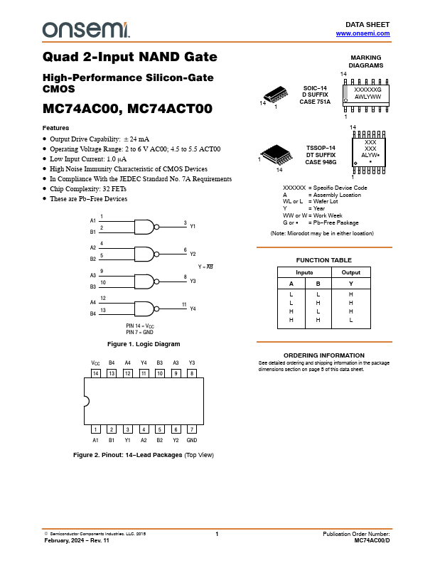
1 A1
2 B1
3 Y1
4 A2
5 B2
9 A3
10 B3
6 Y2 Y = AB
8 Y3
12 A4
13 B4
11 Y4
PIN 14 = VCC PIN 7 = GND
Figure 1. Logic Diagram
VCC B4 A4 Y4 B3 A3 Y3 14 13 12 11 10 9 8
DATA SHEET .onsemi.
MARKING DIAGRAMS
14 1
SOIC- 14 D SUFFIX CASE 751A
XXXXXXG AWLYWW
1 14
1 14
TSSOP- 14 DT SUFFIX CASE 948G
XXX XXX ALYWG
XXXXXX = Specific Device Code
= Assembly Location
WL or L = Wafer Lot
=...