MC74ACT11
MC74ACT11 is Triple 3-Input AND Gate manufactured by onsemi.
MC74AC11, MC74ACT11 co Triple 3-Input t AND Gate
- Outputs Source/Sink 24 m A
- ′ACT11 Has TTL patible Inputs m w w w
.D
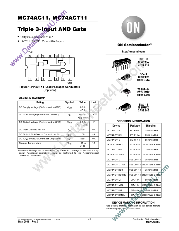
VCC 14 13 12 11 10 9 8 a
S a t e e h
4U
. http://onsemi.
PDIP- 14 N SUFFIX CASE 646
14 1 1 2 3 4 5 6 7 GND 14
Figure 1. Pinout: 14- Lead Packages Conductors (Top View) MAXIMUM RATINGS-
Rating DC Supply Voltage (Referenced to GND) DC Input Voltage (Referenced to GND) DC Output Voltage (Referenced to GND) DC Input Current, per Pin DC Output Sink/Source Current, per Pin DC VCC or GND Current per Output Pin Storage Temperature Symbol VCC Vin Vout Iin Value
- 0.5 to +7.0
- 0.5 to VCC +0.5
- 0.5 to VCC +0.5 ±20 ±50 ±50
- 65 to +150 Unit V V V
Iout
- Maximum Ratings are those values beyond which damage to the device may occur. Functional operation should be restricted to the Remended Operating Conditions. w w w
.D
Tstg t a
S a e h m A m A m A °C t e
U 4
14 14 Device
.c
1 m o
SO- 14 D SUFFIX CASE 751A
TSSOP- 14 DT SUFFIX CASE 948G
EIAJ- 14 M SUFFIX CASE 965
ORDERING INFORMATION
Package PDIP- 14 PDIP- 14 SOIC- 14 SOIC- 14 SOIC- 14 SOIC- 14 TSSOP- 14 Shipping 25 Units/Rail 25 Units/Rail 55 Units/Rail 2500 Tape & Reel 55 Units/Rail 2500 Tape & Reel 96 Units/Rail
MC74AC11N MC74ACT11N MC74AC11D MC74AC11DR2 MC74ACT11D MC74ACT11DR2 MC74AC11DT MC74AC11DTR2 MC74ACT11DT MC74ACT11DTR2 MC74AC11M MC74AC11MEL MC74ACT11M MC74ACT11MEL
TSSOP- 14 2500 Tape & Reel TSSOP- 14 96 Units/Rail
TSSOP- 14 2500 Tape & Reel EIAJ- 14 EIAJ- 14 EIAJ- 14 EIAJ- 14
2000 Tape & Reel 50 Units/Rail
DEVICE MARKING INFORMATION
See general marking information in the device marking section on page 78 of this data sheet.
Semiconductor ponents Industries, LLC,...