MC74HCT245A
Features
- Output Drive Capability: 15 LSTTL Loads
- Outputs Directly Interface to CMOS, NMOS, and TTL
- Operating Voltage Range: 2.0 to 6.0 V (HC), 4.5 to 5.5 V (HCT)
- Low Input Current: 1 m A
- High Noise Immunity Characteristic of CMOS Devices
- In pliance with the Requirements Defined by JEDEC Standard
No. 7 A
- Chip plexity: 308 FETs or 77 Equivalent Gates
- - Q Suffix for Automotive and Other Applications Requiring Unique
Site and Control Change Requirements; AEC- Q100 Qualified and PPAP Capable
- These Devices are Pb- Free, Halogen Free and are Ro HS pliant
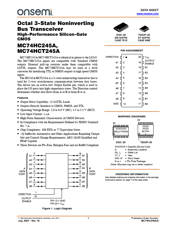
A DATA PORT
2 A1
3 A2
4 A3
5 A4
6 A5
7 A6
A7 8 A8 9
1 DIRECTION
19 OUTPUT ENABLE
PIN 10 = GND PIN 20 = VCC
Figure 1. Logic Diagram
18 B1
17 B2
16 B3
15 B4
14 B5
13 B6
12 B7 11 B8
B DATA PORT
SOIC- 20 DW SUFFIX CASE 751D
TSSOP- 20 DT SUFFIX CASE 948E
PIN ASSIGNMENT
DIRECTION 1 A1 2 A2 3 A3 4 A4 5 A5 6 A6 7 A7 8 A8 9
GND 10
20 VCC
OUTPUT...