MC74HCT32A
Features
- Output Drive Capability: 10 LSTTL Loads
- Outputs Directly Interface to CMOS, NMOS and TTL
- Operating Voltage Range: 2.0 to 6.0 V (HC), 4.5 to 5.5 V (HCT)
- Low Input Current: 1 m A
- High Noise Immunity Characteristic of CMOS Devices
- In pliance With the JEDEC Standard No. 7 A Requirements
- Chip plexity: 48 FETs or 12 Equivalent Gates
- - Q suffix for Automotive and Other Applications Requiring Unique
Site and Control Change Requirements; AEC- Q100 Qualified and PPAP Capable
- These Devices are Pb- Free, Halogen Free/BFR Free and are Ro HS pliant
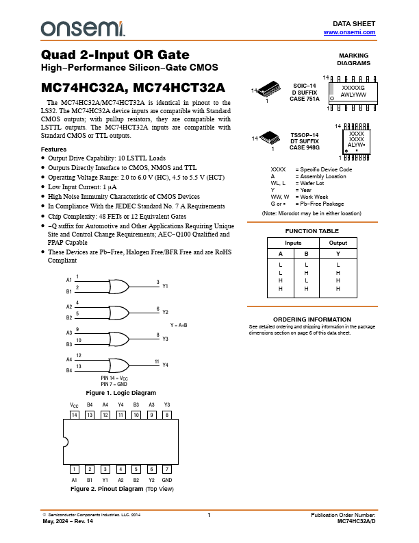
1 A1
2 B1
3 Y1
4 A2
5 B2
9 A3
10 B3
6 Y2 Y = A+B
8 Y3
12 A4
13 B4
PIN 14 = VCC PIN 7 = GND
11 Y4
Figure 1. Logic Diagram
VCC B4 A4 Y4 B3 A3 Y3 14 13 12 11 10 9 8
14 1
MARKING DIAGRAMS
SOIC- 14 D SUFFIX CASE 751A
XXXXXG AWLYWW
14 1
TSSOP- 14 DT SUFFIX CASE 948G
XXXX XXXX ALYWG
XXXX A WL, L Y WW, W G or G
= Specific Device Code = Assembly Location = Wafer Lot = Year = Work Week = Pb- Free Package
(Note:...