MC74HCT365A
Features
- Output Drive Capability: 15 LSTTL Loads
- Outputs Directly Interface to CMOS, NMOS, and TTL
- Operating Voltage Range: 2.0 to 6.0 V (HC), 4.5 to 5.5 V (HCT)
- Low Input Current: 1.0 m A
- High Noise Immunity Characteristic of CMOS Devices
- In pliance with the Requirements Defined by JEDEC Standard
No. 7A
- Chip plexity: 90 FETs or 22.5 Equivalent Gates
- - Q Suffix for Automotive and Other Applications Requiring Unique
Site and Control Change Requirements; AEC- Q100 Qualified and PPAP Capable
- These Devices are Pb- Free, Halogen Free/BFR Free and are Ro HS pliant
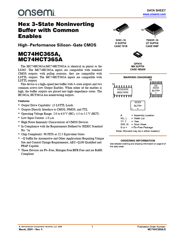
16 1
SOIC- 16 D SUFFIX CASE 751B
1 TSSOP- 16 DT SUFFIX CASE 948F
QFN16 MN SUFFIX CASE 485AW
MARKING DIAGRAMS 16
XXXXXXX AWLYWW
XXXX ALYWG
XXXX ALYWG
A WL, L YY, Y WW, W G or G
= Assembly Location = Wafer Lot = Year = Work Week = Pb- Free Package
(Note: Microdot may be in either location)
ORDERING INFORMATION
See detailed ordering and shipping information on page 8 of this data sheet.
...