MC74HCT74A
MC74HCT74A is Dual D Flip-Flop manufactured by onsemi.
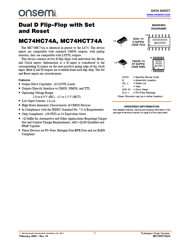
DATA SHEET .onsemi.
Dual D Flip-Flop with Set and Reset
MC74HC74A, MC74HCT74A
The MC74HC74A is identical in pinout to the LS74. The device inputs are patible with standard CMOS outputs; with pullup resistors, they are patible with LSTTL outputs.
This device consists of two D flip- flops with individual Set, Reset, and Clock inputs. Information at a D- input is transferred to the corresponding Q output on the next positive going edge of the clock input. Both Q and Q outputs are available from each flip- flop. The Set and Reset inputs are asynchronous.
Features
- Output Drive Capability: 10 LSTTL Loads
- Outputs Directly Interface to CMOS, NMOS, and TTL
- Operating Voltage...