MC74VHC1G02 Overview
Key Specifications
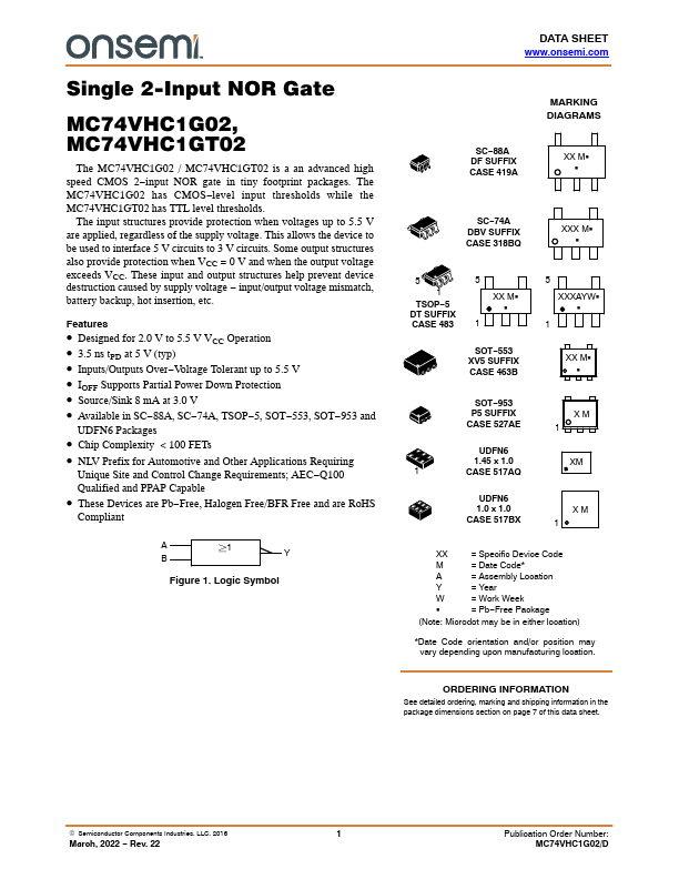
Package: TSSOP
Mount Type: Surface Mount
Pins: 5
Operating Voltage: 5 V
Key Features
- Designed for 2.0 V to 5.5 V VCC Operation
- 3.5 ns tPD at 5 V (typ)
- Inputs/Outputs Over-Voltage Tolerant up to 5.5 V
- IOFF Supports Partial Power Down Protection
- Source/Sink 8 mA at 3.0 V