MC74VHC259
MC74VHC259 is 8-Bit Addressable Latch/1-of-8 Decoder CMOS Logic Level Shifter manufactured by onsemi.
8-Bit Addressable Latch/1-of-8 Decoder CMOS Logic Level Shifter with LSTTL- patible Inputs
The MC74VHC259 is an 8- bit Addressable Latch fabricated with silicon gate CMOS technology. It achieves high speed operation similar to equivalent Bipolar Schottky TTL devices while maintaining CMOS low power dissipation.
The VHC259 is designed for general purpose storage applications in digital systems. The device has four modes of operation as shown in the mode selection table.. In the addressable latch mode, the data on Data In is written into the addressed latch. The addressed latch follows the data input with all non- addressed latches remaining in their previous states. In the memory mode, all latches remain in their previous state and are unaffected by the Data or Address inputs. In the one- of- eight decoding or demultiplexing mode, the addressed output follows the state of Data In with all other outputs in the LOW state. In the Reset mode, all outputs are LOW and unaffected by the address and data inputs. When operating the VHC259 as an addressable latch, changing more than one bit of the address could impose a transient wrong address. Therefore, this should only be done while in the memory mode.
The MC74VHC259 input structure provides protection when voltages up to 7 V are applied, regardless of the supply voltage. This allows the MC74VHC259 to be used to interface 5 V circuits to 3 V circuits.
- High Speed: t PD = 7.6 ns (Typ) at VCC = 5 V
- Low Power Dissipation: ICC = 2 μA (Max) at TA = 25°C
- High Noise Immunity: VNIH = VNIL = 28% VCC
- CMOS- patible Outputs: VOH > 0.8 VCC; VOL < 0.1 VCC @Load
- Power Down Protection Provided on Inputs and Outputs
- Balanced Propagation Delays
- Pin and Function patible with Other Standard Logic Families
- Latchup Performance Exceeds 300 m A
- ESD Performance: HBM > 2000 V
- These Devices are Pb- Free and are Ro HS pliant
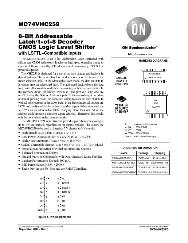
A0 1 A1 2 A2 3 Q0 4 Q1 5 Q2 6 Q3 7 GND 8
16 VCC 15 RESET 14 ENABLE 13 DATA IN 12 Q7 11 Q6 10 Q5 9...