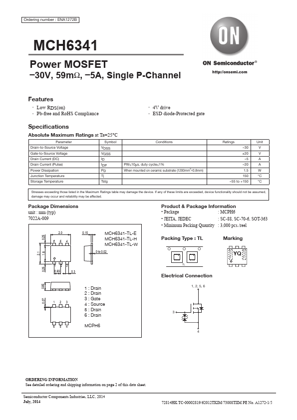
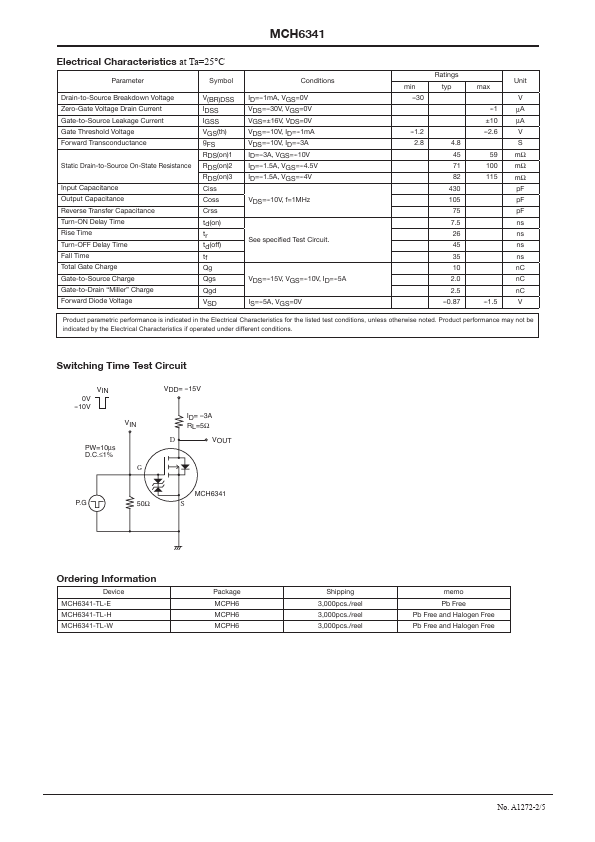
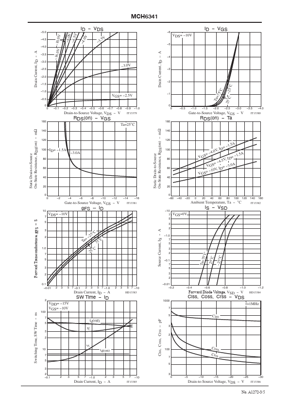
MCH6341 Overview
ENA1272B MCH6341 Power MOSFET 30V, 59mΩ, 5A, Single P-Channel http://onsemi.
MCH6341 Key Features
- Low RDS(on)
- Pb-free and RoHS pliance
- 4V drive
- ESD diode-Protected gate
MCH6341 datasheet by onsemi.
| Part number | MCH6341 |
|---|---|
| Datasheet | MCH6341-ONSemiconductor.pdf |
| File Size | 525.94 KB |
| Manufacturer | onsemi |
| Description | Power MOSFET |
|
|
ENA1272B MCH6341 Power MOSFET 30V, 59mΩ, 5A, Single P-Channel http://onsemi.
| Brand Logo | Part Number | Description | Other Manufacturers |
|---|---|---|---|
| MCH6341 | P-Channel Silicon MOSFET | Sanyo |
| Part Number | Description |
|---|---|
| MCH6342 | Power MOSFET |
| MCH6344 | Power MOSFET |
| MCH6320 | Power MOSFET |
| MCH6321 | P-Channel Power MOSFET |
| MCH6331 | Power MOSFET |
| MCH6336 | P-Channel Power MOSFET |
| MCH6337 | P-Channel Power MOSFET |
| MCH6353 | P-Channel Power MOSFET |
| MCH6001 | RF Transistor |
| MCH6101 | Bipolar Transistor |