MM3Z15VST1
MM3Z15VST1 is Zener Voltage Regulators manufactured by onsemi.
es: http://onsemi.
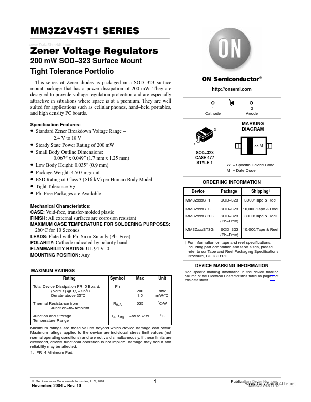
1 Cathode
2 Anode
- Standard Zener Breakdown Voltage Range
- -
- -
- -
- -
2.4 V to 18 V Steady State Power Rating of 200 m W Small Body Outline Dimensions: 0.067″ x 0.049″ (1.7 mm x 1.25 mm) Low Body Height: 0.035″ (0.9 mm) Package Weight: 4.507 mg/unit ESD Rating of Class 3 (>16 k V) per Human Body Model Tight Tolerance VZ Pb- Free Packages are Available
MARKING DIAGRAM xx M
SOD- 323 CASE 477 STYLE 1 xx = Specific Device Code M = Date Code
ORDERING INFORMATION
Device MM3Zxxx ST1 Package SOD- 323 SOD- 323 SOD- 323 (Pb- Free) SOD- 323 (Pb- Free) Shipping† 3000/Tape & Reel 10,000/Tape & Reel 3000/Tape & Reel 10,000/Tape & Reel
Mechanical Characteristics: CASE: Void-free, transfer-molded plastic FINISH: All external surfaces are corrosion resistant MAXIMUM CASE TEMPERATURE FOR SOLDERING PURPOSES:
MM3Zxxx ST3 MM3Zxxx ST1G MM3Zxxx ST3G
260°C for 10 Seconds LEADS: Plated with Pb- Sn or Sn only (Pb- Free) POLARITY: Cathode indicated by polarity band FLAMMABILITY RATING: UL 94 V- 0 MOUNTING POSITION: Any
MAXIMUM RATINGS
Rating Total Device Dissipation FR- 5 Board, (Note 1) @ TA = 25°C Derate above 25°C Thermal Resistance from Junction- to- Ambient Junction and Storage Temperature Range Symbol PD 200 1.5 Rq JA TJ, Tstg 635
- 65 to +150 m W m W/°C °C/W °C Max Unit
†For information on tape and reel specifications, including part orientation and tape sizes, please refer to our Tape and Reel Packaging Specifications Brochure, BRD8011/D.
DEVICE MARKING INFORMATION
See specific marking information in the device marking column of the Electrical Characteristics table on page 2 of this data sheet.
Maximum ratings are those values beyond which device damage can occur. Maximum ratings applied to the device are individual stress limit values (not normal operating conditions) and are not valid simultaneously. If these limits are exceeded, device functional operation is not implied, damage may occur and reliability may be affected. 1. FR- 4 Minimum Pad.
© Semiconductor...