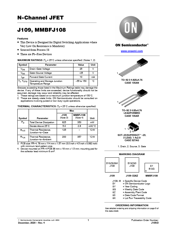
MMBFJ108 Overview
Key Features
- This Device is Designed for Digital Switching Applications where Very Low On Resistance is Mandatory
- Sourced from Process 58
- These are Pb-Free Devices
| Part | MMBFJ108 |
|---|---|
| Description | N-Channel JFET |
| Manufacturer | onsemi |
| Size | 439.69 KB |
| Part Number | Manufacturer | Description |
|---|---|---|
| MMBFJ108 | Fairchild Semiconductor | N-Channel Switch |
| MMBFJ109 | Fairchild Semiconductor | N-Channel Switch |