MMDL914T1
MMDL914T1 is High-Speed Switching Diode manufactured by onsemi.
Features
- Pb- Free Package is Available http://onsemi.
MAXIMUM RATINGS
Rating Reverse Voltage Forward Current Peak Forward Surge Current Symbol VR IF IFM(surge) Value 100 200 500 Unit Vdc m Adc m Adc
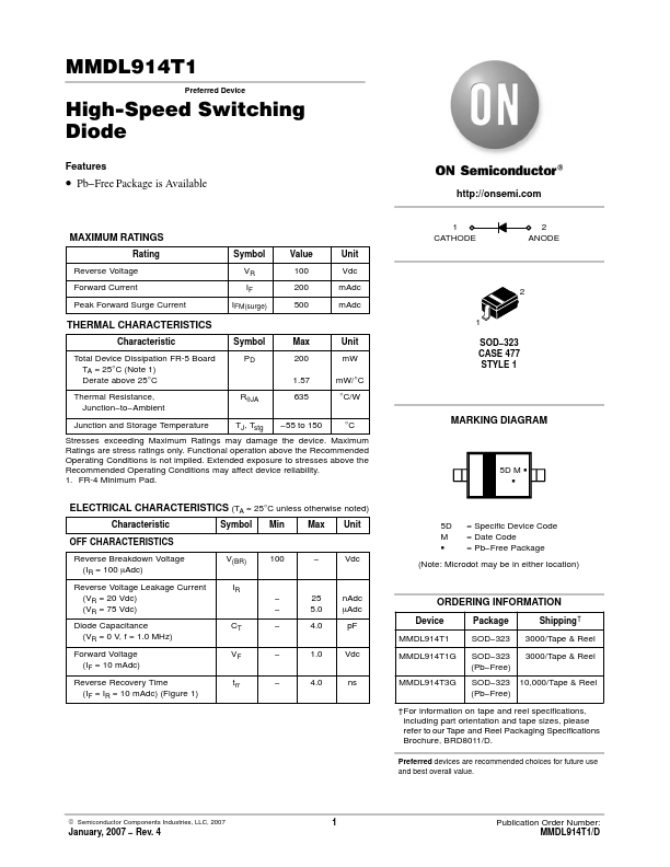
1 CATHODE
2 ANODE
THERMAL CHARACTERISTICS
Characteristic Total Device Dissipation FR-5 Board TA = 25°C (Note 1) Derate above 25°C Thermal Resistance, Junction- to- Ambient Junction and Storage Temperature Symbol PD Max 200 1.57 Rq JA TJ, Tstg 635
- 55 to 150 Unit m W m W/°C °C/W °C
1 SOD- 323 CASE 477 STYLE 1
MARKING DIAGRAM
Stresses exceeding Maximum Ratings may damage the device. Maximum Ratings are stress ratings only. Functional operation above the Remended Operating Conditions is not implied. Extended exposure to stresses above the Remended Operating Conditions may affect device reliability. 1. FR-4 Minimum Pad.
5D M G G
ELECTRICAL CHARACTERISTICS (TA = 25°C unless otherwise noted)
Characteristic OFF CHARACTERISTICS Reverse Breakdown Voltage (IR = 100 m Adc) Reverse Voltage Leakage Current (VR = 20 Vdc) (VR = 75 Vdc) Diode Capacitance (VR = 0 V, f = 1.0 MHz) Forward Voltage (IF = 10 m Adc) Reverse Recovery Time (IF = IR = 10 m Adc) (Figure 1) V(BR) IR
- - CT VF trr
- -
- 25 5.0 4.0 1.0 4.0 n Adc m Adc p F Vdc ns 100
- Vdc Symbol Min Max Unit 5D M G = Specific Device Code = Date Code = Pb- Free Package
(Note: Microdot may be in either location)
ORDERING INFORMATION
Device MMDL914T1 MMDL914T1G MMDL914T3G Package SOD- 323 SOD- 323 (Pb- Free) SOD- 323 (Pb- Free) Shipping † 3000/Tape & Reel 3000/Tape & Reel 10,000/Tape & Reel
†For information on tape and reel specifications, including part orientation and tape sizes, please refer to our Tape and Reel Packaging Specifications Brochure, BRD8011/D.
Preferred devices are remended choices for future use and best overall value.
© Semiconductor ponents Industries, LLC, 2007
January, 2007
- Rev. 4
Publication Order Number: MMDL914T1/D
820 W +10 V 2.0 k 100 m H 0.1 m F D.U.T. 50 W OUTPUT PULSE GENERATOR 50 W INPUT...