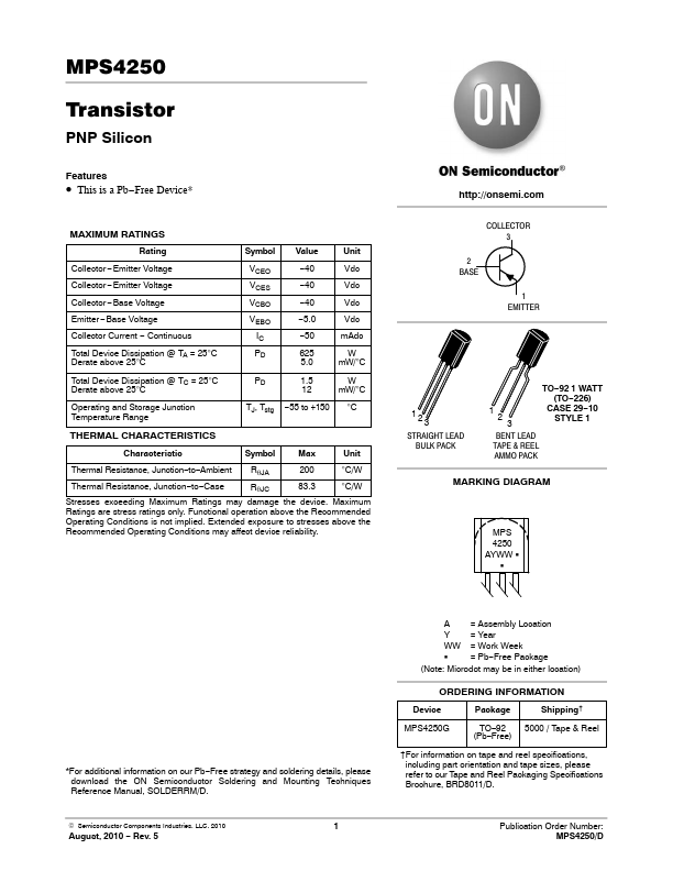
The following content is an automatically extracted verbatim text
from the original manufacturer datasheet and is provided for reference purposes only.
View original datasheet text
MPS4250
Transistor
PNP Silicon
Features
• This is a Pb−Free Device*
MAXIMUM RATINGS
Rating
Symbol Value
Unit
Collector −Emitter Voltage Collector −Emitter Voltage Collector −Base Voltage Emitter −Base Voltage Collector Current − Continuous Total Device Dissipation @ TA = 25°C Derate above 25°C
VCEO VCES VCBO VEBO
IC PD
−40 −40 −40 −5.0 −50 625 5.0
Vdc Vdc Vdc Vdc mAdc W mW/°C
Total Device Dissipation @ TC = 25°C PD 1.5 W
Derate above 25°C
12 mW/°C
Operating and Storage Junction Temperature Range
TJ, Tstg −55 to +150 °C
THERMAL CHARACTERISTICS
Characteristic
Symbol
Max
Unit
Thermal Resistance, Junction−to−Ambient RqJA
200 °C/W
Thermal Resistance, Junction−to−Case
RqJC
83.3 °C/W
Stresses exceeding Maximum Ratings may damage the device.