MPS5179
Features
- Pb- Free Packages are Available-
MAXIMUM RATINGS
Rating Collector
- Emitter Voltage Collector
- Base Voltage Emitter
- Base Voltage Collector Current
- Continuous Total Device Dissipation @ TA = 25°C Derate above 25°C Total Device Dissipation @ TC = 25°C Derate above 25°C Storage Temperature Range Symbol VCEO VCBO VEBO IC PD PD Tstg Value 12 20 2.5 50 200 1.14 300 1.71
- 55 to +150 Unit Vdc Vdc Vdc m Adc W m W/°C W m W/°C °C http://onsemi.
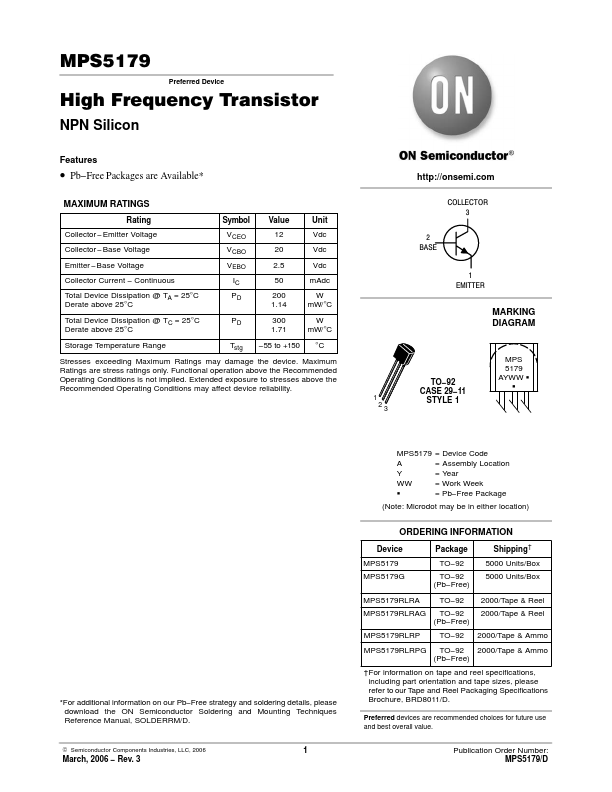
COLLECTOR 3 2 BASE 1 EMITTER
MARKING DIAGRAM
Stresses exceeding Maximum Ratings may damage the device. Maximum Ratings are stress ratings only. Functional operation above the Remended Operating Conditions is not implied. Extended exposure to stresses above the Remended Operating Conditions may affect device reliability.
1 2 3
TO- 92 CASE 29- 11 STYLE 1
MPS 5179 AYWW G G
MPS5179 A Y WW G
= Device Code = Assembly Location = Year = Work Week = Pb- Free Package
(Note: Microdot may be in either location)
ORDERING INFORMATION
Device MPS5179...