MPS6560
Features
- Pb- Free Package is Available-
MAXIMUM RATINGS
Rating Collector
- Emitter Voltage Collector
- Base Voltage Emitter
- Base Voltage Collector Current
- Continuous Total Device Dissipation @ TA = 25°C Derate above 25°C Total Device Dissipation @ TC = 25°C Derate above 25°C Operating and Storage Junction Temperature Range Symbol VCEO VCBO VEBO IC PD PD TJ, Tstg Value 25 25 5.0 500 625 5.0 1.5 12
- 55 to +150 Unit Vdc Vdc Vdc m Adc W m W/°C W m W/°C °C http://onsemi.
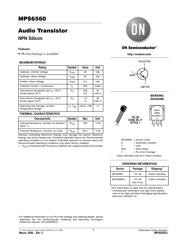
COLLECTOR 3 2 BASE 1 EMITTER
MARKING DIAGRAM
THERMAL CHARACTERISTICS
Characteristic Thermal Resistance, Junction- to- Ambient (Note 1) Thermal Resistance, Junction- to- Case Symbol Rq JA Rq JC Max 200 83.3 Unit °C/W °C/W
1 2 3
TO- 92 CASE 29- 11 STYLE 1
MPS 6560 AYWW G G
Stresses exceeding Maximum Ratings may damage the device. Maximum Ratings are stress ratings only. Functional operation above the Remended Operating Conditions is not implied. Extended exposure to stresses above the Remended Operating Conditions may affect...