MPS6652
Features
- Voltage and Current are Negative for PNP Transistors
- Pb- Free Packages are Available-
MAXIMUM RATINGS
Rating Collector
- Emitter Voltage MPS6601/6651 MPS6602/6652 Collector
- Base Voltage MPS6601/6651 MPS6602/6652 Emitter
- Base Voltage Collector Current
- Continuous Total Device Dissipation @ TA = 25°C Derate above 25°C Total Device Dissipation @ TC = 25°C Derate above 25°C Operating and Storage Junction Temperature Range VEBO IC PD PD TJ, Tstg VCBO 25 30 4.0 1000 625 5.0 1.5 12
- 55 to +150 Vdc m Adc W m W/°C W m W/°C °C Symbol VCEO 25 40 Vdc Value Unit Vdc 2 BASE http://onsemi.
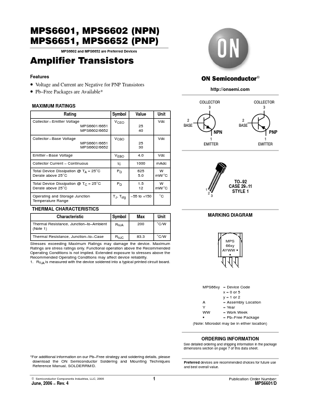
COLLECTOR 3 2 BASE NPN 1 EMITTER PNP 1 EMITTER COLLECTOR 3
1 2 3
TO- 92 CASE 29- 11 STYLE 1
THERMAL CHARACTERISTICS
Characteristic Thermal Resistance, Junction- to- Ambient (Note 1) Thermal Resistance, Junction- to- Case Symbol Rq JA Rq JC Max 200 83.3 Unit °C/W °C/W
MARKING DIAGRAM
Stresses exceeding Maximum Ratings may damage the device. Maximum Ratings are stress ratings only. Functional operation...