MPS6725
Features http://onsemi.
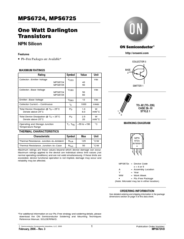
COLLECTOR 3 BASE 2
- Pb- Free Packages are Available-
MAXIMUM RATINGS
Rating Collector
- Emitter Voltage MPS6724 MPS6725 Collector
- Base Voltage MPS6724 MPS6725 Emitter
- Base Voltage Collector Current
- Continuous Total Device Dissipation @ TA = 25°C Derate above 25°C Total Device Dissipation @ TC = 25°C Derate above 25°C Operating and Storage Junction Temperature Range VEBO IC PD PD TJ, Tstg VCBO 50 60 12 1000 1.0 8.0 2.5 20
- 55 to +150 Vdc m Adc W m W/°C W m W/°C °C 1 2 Symbol VCEO 40 50 Vdc Value Unit Vdc
EMITTER 1
TO- 92 (TO- 226) CASE 29- 10 STYLE 1 3
MARKING DIAGRAM
THERMAL CHARACTERISTICS
Characteristic Thermal Resistance, Junction- to- Ambient Thermal Resistance, Junction- to- Case Symbol Rq JA Rq JC Max 125 50 Unit °C/W °C/W MPS 672x AYWW G G
Maximum ratings are those values beyond which device damage can occur. Maximum ratings applied to the device are individual stress limit values (not normal operating conditions) and are not valid simultaneously. If these...