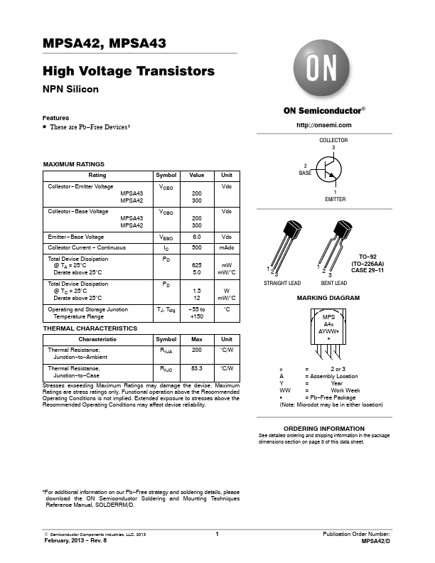
MPSA42
Overview
- These are Pb-Free Devices*
| Part | MPSA42 |
|---|---|
| Description | High Voltage Transistors |
| Category | Transistor |
| Manufacturer | onsemi |
| Size | 101.48 KB |
| Part Number | Manufacturer | Description |
|---|---|---|
| MPSA42 | Unisonic Technologies | NPN TRANSISTOR |
| MPSA42 | Philips Semiconductors | NPN high-voltage transistors |
| MPSA42M | Dc Components | NPN EPITAXIAL PLANAR TRANSISTOR |
| MPSA42 | General Semiconductor | Small Signal Transistors |
| MPSA42 | Taitron Components | Small Signal High Voltage Transistors |