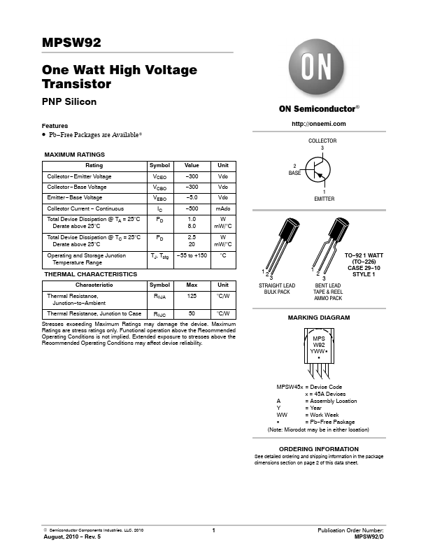
The following content is an automatically extracted verbatim text
from the original manufacturer datasheet and is provided for reference purposes only.
View original datasheet text
MPSW92
One Watt High Voltage Transistor
PNP Silicon
Features
• Pb−Free Packages are Available*
MAXIMUM RATINGS
Rating
Symbol
Value
Unit
Collector −Emitter Voltage Collector −Base Voltage Emitter −Base Voltage Collector Current − Continuous Total Device Dissipation @ TA = 25°C
Derate above 25°C
VCEO VCBO VEBO
IC PD
−300
−300
−5.0
−500
1.0 8.0
Vdc
Vdc
Vdc
mAdc
W mW/°C
Total Device Dissipation @ TC = 25°C Derate above 25°C
PD
2.5 W 20 mW/°C
Operating and Storage Junction Temperature Range
TJ, Tstg − 55 to +150
°C
THERMAL CHARACTERISTICS
Characteristic
Symbol
Max
Unit
Thermal Resistance, Junction−to−Ambient
RqJA
125 °C/W
Thermal Resistance, Junction to Case RqJC
50 °C/W
Stresses exceeding Maximum Ratings may damage the device.