MSC3930-BT1
MSC3930- BT1
Preferred Device
NPN RF Amplifier Transistor
- Pb- Free Package is Available http://onsemi.
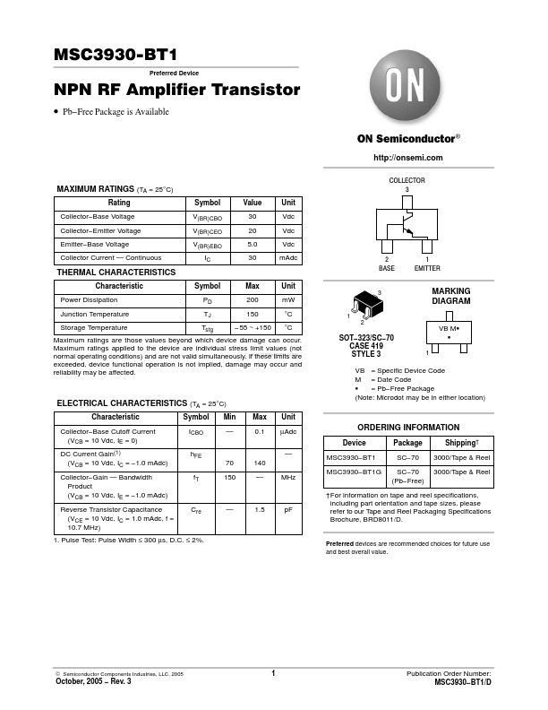
COLLECTOR 3 Symbol V(BR)CBO V(BR)CEO V(BR)EBO IC Value 30 20 5.0 30 Unit Vdc Vdc Vdc m Adc 2 BASE
MAXIMUM RATINGS (TA = 25°C)
Rating Collector- Base Voltage Collector- Emitter Voltage Emitter- Base Voltage Collector Current
- Continuous
THERMAL CHARACTERISTICS
Characteristic Power Dissipation Junction Temperature Storage Temperature Symbol PD TJ Tstg Max 200 150
- 55 ~ +150 Unit m W °C °C
1 2
1 EMITTER
MARKING DIAGRAM
VB MG G 1
Maximum ratings are those values beyond which device damage can occur. Maximum ratings applied to the device are individual stress limit values (not .. normal operating conditions) and are not valid simultaneously. If these limits are exceeded, device functional operation is not implied, damage may occur and reliability may be affected.
SOT- 323/SC- 70 CASE 419 STYLE 3
ELECTRICAL CHARACTERISTICS (TA = 25°C)
Characteristic Collector- Base Cutoff Current (VCB...