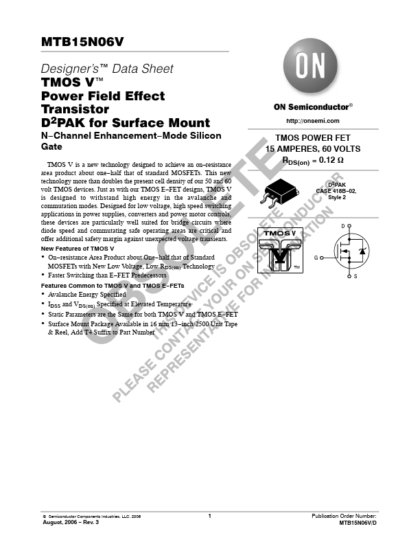
Datasheet4U Logo Datasheet4U.com

MTB15N06V - Power Field Effect Transistor

Key Features

  • of TMOS V.
  • On.
  • resistance Area Product about One.
  • half that of Standard MOSFETs with New Low Voltage, Low RDS(on) Technology.
  • Faster Switching than E.
  • FET Predecessors Features Common to TMOS V and TMOS E.
  • FETs.
  • Avalanche Energy Specified.
  • IDSS and VDS(on) Specified at Elevated Temperature.
  • Static Parameters are the Same for both TMOS V and TMOS E.
  • FET.
  • Surface Mount Package Available in 16 mm 13.
  • inc.

📥 Download Datasheet

Datasheet Details

Part number MTB15N06V
Manufacturer onsemi
File Size 270.29 KB
Description Power Field Effect Transistor
Datasheet download datasheet MTB15N06V Datasheet

Full PDF Text Transcription (Reference)

The following content is an automatically extracted verbatim text from the original manufacturer datasheet and is provided for reference purposes only.

View original datasheet text
MTB15N06V Designer’s™ Data Sheet TMOS V™ Power Field Effect Transistor D2PAK for Surface Mount N−Channel Enhancement−Mode Silicon Gate TMOS V is a new technology designed to achieve an on−resistance area product about one−half that of standard MOSFETs. This new technology more than doubles the present cell density of our 50 and 60 volt TMOS devices. Just as with our TMOS E−FET designs, TMOS V is designed to withstand high energy in the avalanche and commutation modes. Designed for low voltage, high speed switching applications in power supplies, converters and power motor controls, these devices are particularly well suited for bridge circuits where diode speed and commutating safe operating areas are critical and offer additional safety margin against unexpected voltage transients.