MUN2215T1G
Features
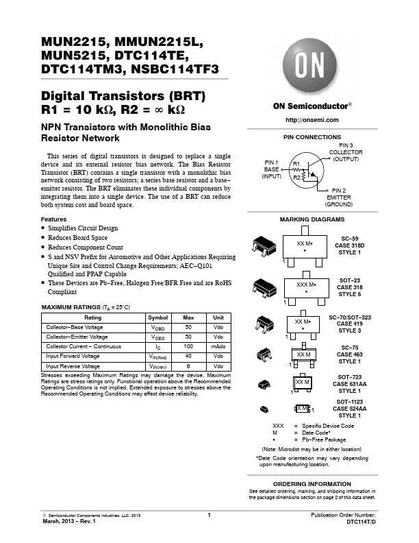
PIN 1 BASE (INPUT) http://onsemi. PIN CONNECTIONS
PIN 3 COLLECTOR (OUTPUT)
R1 R2
PIN 2 EMITTER (GROUND)
- -
- -
- MARKING DIAGRAMS
SC- 59 CASE 318D STYLE 1
Simplifies Circuit Design Reduces Board Space Reduces ponent Count S and NSV Prefix for Automotive and Other Applications Requiring Unique Site and Control Change Requirements; AEC- Q101 Qualified and PPAP Capable These Devices are Pb- Free, Halogen Free/BFR Free and are Ro HS pliant
XX MG G 1
XXX MG G 1
SOT- 23 CASE 318 STYLE 6
MAXIMUM RATINGS (TA = 25°C)
Rating Collector- Base Voltage Collector- Emitter Voltage Collector Current
- Continuous Input Forward Voltage Input Reverse Voltage Symbol VCBO VCEO IC VIN(fwd) VIN(rev) Max 50 50 100 40 6 Unit Vdc Vdc m Adc Vdc Vdc
XX MG G 1 XX M 1 XX M 1 XM 1 XXX M G
SC- 70/SOT- 323 CASE 419 STYLE 3 SC- 75 CASE 463 STYLE 1 SOT- 723 CASE 631AA STYLE 1 SOT- 1123 CASE 524AA STYLE 1
Stresses exceeding Maximum Ratings may damage the device. Maximum Ratings are stress ratings only....