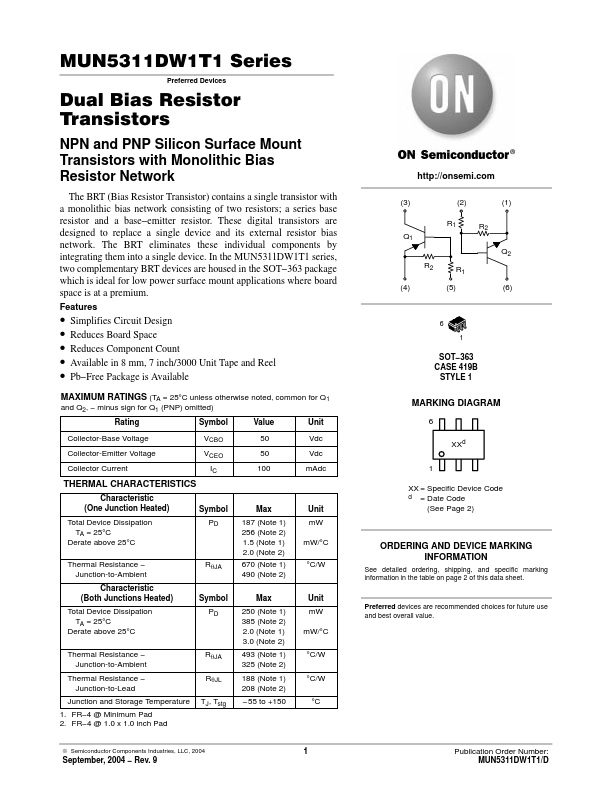
MUN5311DW1T1
Features
- Simplifies Circuit Design
- Reduces Board Space
- Reduces ponent Count
- Available in 8 mm, 7 inch/3000 Unit Tape and Reel
- Pb- Free Package is Available
MAXIMUM RATINGS (TA = 25°C unless otherwise noted, mon for Q1 and Q2,
- minus sign for Q1 (PNP) omitted)
Rating
Symbol
Value
Unit
Collector-Base Voltage
VCBO
Vdc
Collector-Emitter Voltage
VCEO
Vdc
Collector Current
IC 100 m Adc
THERMAL CHARACTERISTICS
Characteristic (One Junction Heated)
Total Device Dissipation TA = 25°C
Derate above 25°C
Symbol PD
Thermal Resistance
- Junction-to-Ambient
Characteristic (Both Junctions Heated)
Total Device Dissipation TA = 25°C
Derate above 25°C
Rq JA
Symbol PD
Thermal Resistance
- Junction-to-Ambient
Thermal Resistance
- Junction-to-Lead
Junction and Storage Temperature
1. FR- 4 @ Minimum Pad 2. FR- 4 @ 1.0 x 1.0 inch...