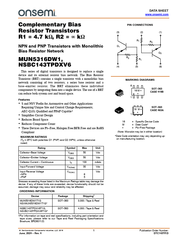
MUN5316DW1
Features
- S and NSV Prefix for Automotive and Other Applications
Requiring Unique Site and Control Change Requirements;
AEC-Q101 Qualified and PPAP Capable-
- Simplifies Circuit Design
- Reduces Board Space
- Reduces ponent Count
- These Devices are Pb- Free, Halogen Free/BFR Free and are Ro HS pliant
MAXIMUM RATINGS (TA = 25C both polarities Q1 (PNP) and Q2 (NPN), unless otherwise noted)
Rating
Symbol
Max
Unit
Collector- Base Voltage
Collector- Emitter Voltage
Collector Current
- Continuous
Input Forward Voltage
Input Reverse Voltage
- NPN
- PNP
VCBO
VCEO
VIN(fwd)
VIN(rev) 6 5
Vdc Vdc m Adc Vdc Vdc
Stresses exceeding those listed in the Maximum Ratings table may damage the device. If any of these limits are exceeded, device functionality should not be assumed, damage may occur and reliability may be affected.
ORDERING INFORMATION
Device
Package
Shipping†
MUN5316DW1T1G NSVMUN5316DW1T1G-
SOT- 363
3,000 / Tape & Reel
NSBC143TPDXV6T1G, NSVBC143TPDXV6T1G-...