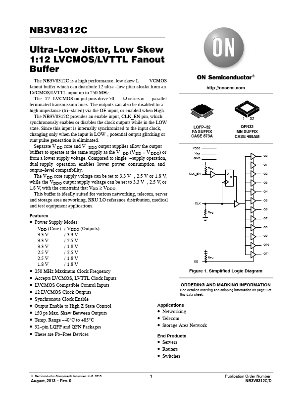
Datasheet4U Logo Datasheet4U.com

NB3V8312C - Ultra-Low Jitter Low Skew 1:12 LVCMOS - LVTTL Fanout Buffer

Datasheet Summary

Description

Pin 1, 5, 8, 12, 16, 17, 21, 25, 29 2, 7 3 Name GND VDD CLK_EN I/O Power Power Input High Open Default Description Ground, Negative Power Supply Positive Supply for Core and Inputs Synchronous Clock Enable Input.

When High, outputs are enabled.

When Low, outputs are disabled Low.

Features

  • http://onsemi. com 1 LQFP.
  • 32 FA SUFFIX CASE 873A VDDO VDD GND RPU CLK_EN D Q 32 QFN32 MN SUFFIX CASE 488AM Q0 Q1 Q2 Q3 Q4 Q5 Q6 Q7 Q8 Q9 Q10 Q11 CLK RPD.
  • Power Supply Modes:.
  • VDD (Core) / VDDO (Outputs) 3.3 V / 3.3 V 3.3 V / 2.5 V 3.3 V / 1.8 V 2.5 V / 2.5 V 2.5 V / 1.8 V 1.8 V / 1.8 V 250 MHz Maximum Clock Frequency Accepts LVCMOS, LVTTL Clock Inputs LVCMOS Compatible Contr.

📥 Download Datasheet

Datasheet preview – NB3V8312C

Datasheet Details

Part number NB3V8312C
Manufacturer ON Semiconductor
File Size 292.04 KB
Description Ultra-Low Jitter Low Skew 1:12 LVCMOS - LVTTL Fanout Buffer
Datasheet download datasheet NB3V8312C Datasheet
Additional preview pages of the NB3V8312C datasheet.
Other Datasheets by ON Semiconductor

Full PDF Text Transcription

Click to expand full text
NB3V8312C Ultra-Low Jitter, Low Skew 1:12 LVCMOS/LVTTL Fanout Buffer The NB3V8312C is a high performance, low skew L VCMOS fanout buffer which can distribute 12 ultra −low jitter clocks from an LVCMOS/LVTTL input up to 250 MHz. The 12 LVCMOS output pins drive 50 W series or parallel terminated transmission lines. The outputs can also be disabled to a high impedance (tri−stated) via the OE input, or enabled when High. The NB3V8312C provides an enable input, CLK_EN pin, which synchronously enables or disables the clock outputs while in the LOW state. Since this input is internally synchronized to the input clock, changing only when the input is LOW , potential output glitching or runt pulse generation is eliminated.
Published: |