NBXDBA017
NBXDBA017 is Clock Oscillator manufactured by onsemi.
NBXDBB017, NBXDBA017, NBXHBA017, NBXSBA017 3.3 V, 156.25 MHz / 312.5 MHz LVPECL Clock Oscillator
The single and dual frequency crystal oscillator (XO) is designed to meet today’s requirements for 3.3 V LVPECL clock generation applications. The device uses a high Q fundamental crystal and Phase Lock Loop (PLL) multiplier to provide selectable 156.25 MHz or 312.5 MHz, ultra low jitter and phase noise LVPECL differential output. This device is a member of ON Semiconductor’s Pure Edget clock family that provides accurate and precision clock solutions. Available in 5 mm x 7 mm SMD (CLCC) package on 16 mm tape and reel in quantities of 1,000. Frequency stability options available as either 50 PPM NBXDBA017, NBXSBA017, NBXHBA017 (Industrial Temperature Range) or 20 PPM NBXDBB017 (mercial Temperature Range).
Features http://onsemi.
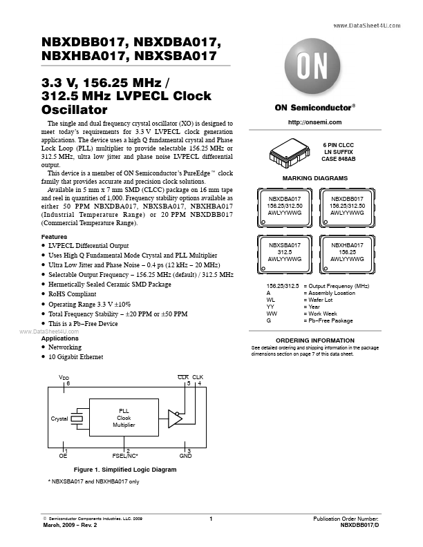
6 PIN CLCC LN SUFFIX CASE 848AB
MARKING DIAGRAMS
NBXDBA017 156.25/312.50 AWLYYWWG NBXDBB017 156.25/312.50 AWLYYWWG
- -
- -
- -
- -
- LVPECL Differential Output Uses High Q Fundamental Mode Crystal and PLL Multiplier Ultra Low Jitter and Phase Noise
- 0.4 ps (12 k Hz
- 20 MHz) Selectable Output Frequency
- 156.25 MHz (default) / 312.5 MHz Hermetically Sealed Ceramic SMD Package Ro HS pliant Operating Range 3.3 V ±10% Total Frequency Stability
- ±20 PPM or ±50 PPM This is a Pb- Free Device
NBXSBA017 312.5 AWLYYWWG
NBXHBA017 156.25 AWLYYWWG
156.25/312.5 A WL YY WW G
= Output Frequency (MHz) = Assembly Location = Wafer Lot = Year = Work Week = Pb- Free Package
..
Applications
- Networking
- 10 Gigabit Ethernet
VDD 6 CLK CLK 5 4
ORDERING INFORMATION
See detailed ordering and shipping information in the package dimensions section on page 7 of this data sheet.
Crystal
PLL Clock Multiplier
1 OE
2 FSEL/NC-...