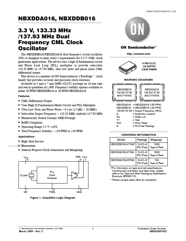
NBXDDB016 Description
1 2 3 4 5 6 Symbol OE FSEL GND CLK CLK VDD I/O LVTTL/LVCMOS Control Input Control Input Power Supply CML Output CML Output Power Supply Description Output Enable Pin. When left floating pin defaults to logic HIGH and output is active. See OE pin description Table.
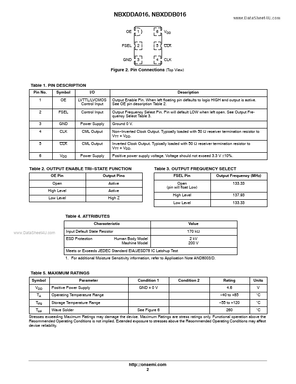
NBXDDB016 Key Features
- 0.4 ps (12 kHz
- 20 MHz) Selectable Output Frequency
- 133.33 MHz (default)/137.93 MHz Hermetically Sealed Ceramic SMD Package RoHS pliant Operating Range 3.3 V ±10% Total Fre
- ±20 PPM or ±50 PPM