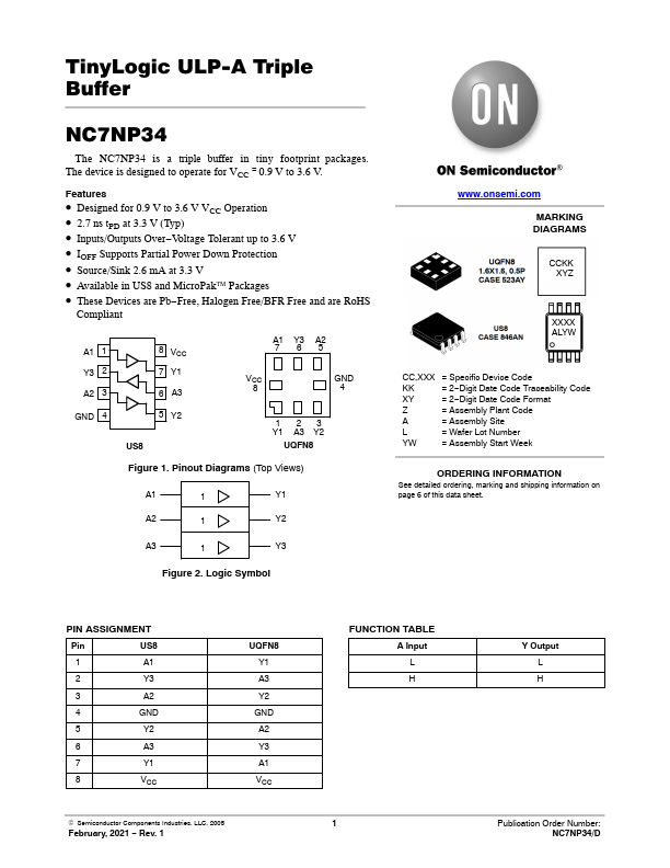
Datasheet4U Logo Datasheet4U.com

NC7NP34 - TinyLogic ULP-A Triple Buffer

Features

  • Designed for 0.9 V to 3.6 V VCC Operation.
  • 2.7 ns tPD at 3.3 V (Typ).
  • Inputs/Outputs Over.
  • Voltage Tolerant up to 3.6 V.
  • IOFF Supports Partial Power Down Protection.
  • Source/Sink 2.6 mA at 3.3 V.
  • Available in US8 and MicroPak™ Packages.
  • These Devices are Pb.
  • Free, Halogen Free/BFR Free and are RoHS Compliant A1 1 Y3 2 A2 3 GND 4 8 VCC 7 Y1 6 A3 A1 Y3 A2 765 VCC GND 8 4 5 Y2 US8 123 Y1 A3 Y2 UQFN8 Figure 1. Pin.

📥 Download Datasheet

Datasheet preview – NC7NP34

Datasheet Details

Part number NC7NP34
Manufacturer onsemi
File Size 528.30 KB
Description TinyLogic ULP-A Triple Buffer
Datasheet download datasheet NC7NP34 Datasheet
Additional preview pages of the NC7NP34 datasheet.
Other Datasheets by ON Semiconductor

Full PDF Text Transcription

Click to expand full text
TinyLogic ULP-A Triple Buffer NC7NP34 The NC7NP34 is a triple buffer in tiny footprint packages. The device is designed to operate for VCC = 0.9 V to 3.6 V. Features • Designed for 0.9 V to 3.6 V VCC Operation • 2.7 ns tPD at 3.3 V (Typ) • Inputs/Outputs Over−Voltage Tolerant up to 3.6 V • IOFF Supports Partial Power Down Protection • Source/Sink 2.6 mA at 3.3 V • Available in US8 and MicroPak™ Packages • These Devices are Pb−Free, Halogen Free/BFR Free and are RoHS Compliant A1 1 Y3 2 A2 3 GND 4 8 VCC 7 Y1 6 A3 A1 Y3 A2 765 VCC GND 8 4 5 Y2 US8 123 Y1 A3 Y2 UQFN8 Figure 1. Pinout Diagrams (Top Views) A1 1 Y1 A2 1 Y2 A3 1 Y3 Figure 2. Logic Symbol www.onsemi.
Published: |