NC7SP57
Features
- Designed for 0.9 V to 3.6 V VCC Operation
- 3.4 ns t PD at 3.3 V (Typ)
- Inputs/Outputs Over- Voltage Tolerant up to 3.6 V
- IOFF Supports Partial Power Down Protection
- Source/Sink 2.6 m A at 3.3 V
- Available in SC- 88 and Micro Pak™ Packages
- These Devices are Pb- Free, Halogen Free/BFR Free and are Ro HS pliant
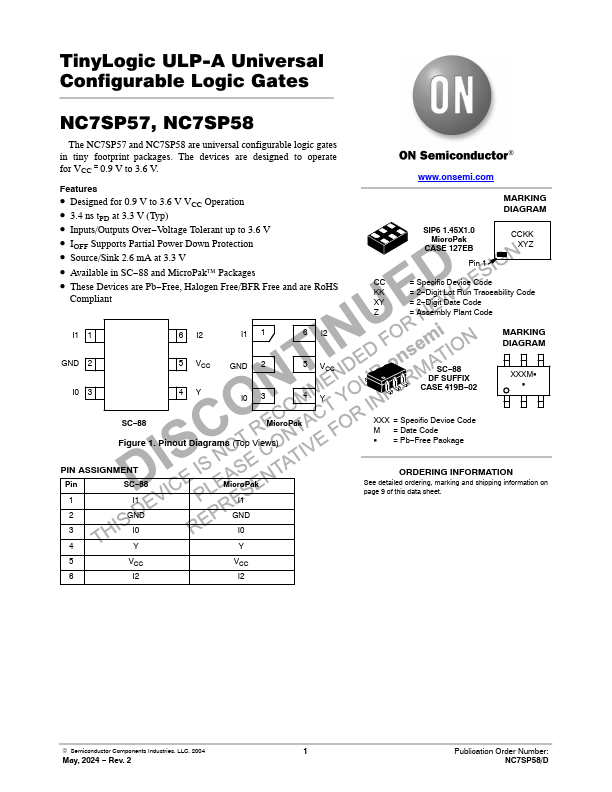
I1 1
6 I2
I1 1
6 I2
GND 2 I0 3
5 VCC
GND 2
5 VCC
4Y
I0 3
4Y
SC- 88
Micro Pak
Figure 1. Pinout Diagrams (Top Views)
PIN ASSIGNMENT
Pin
SC- 88
I1
I0
I2
Micro Pak I1
GND I0 Y
VCC I2
.onsemi.
MARKING DIAGRAM
SIP6 1.45X1.0 Micro Pak
CASE 127EB
Pin 1
CCKK...