NC7WZ241
Description
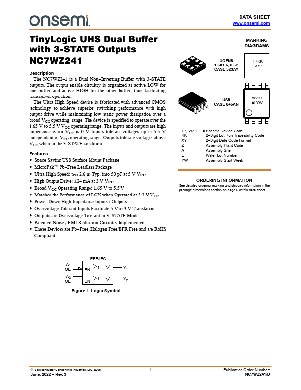
The NC7WZ241 is a Dual Non- Inverting Buffer with 3- STATE outputs. The output enable circuitry is organized as active LOW for one buffer and active HIGH for the other buffer, thus facilitating transceiver operation.
The Ultra High Speed device is fabricated with advanced CMOS technology to achieve superior switching performance with high output drive while maintaining low static power dissipation over a broad VCC operating range. The device is specified to operate over the 1.65 V to 5.5 V VCC operating range. The inputs and outputs are high impedance when VCC is 0 V. Inputs tolerate voltages up to 5.5 V independent of VCC operating range. Outputs tolerate voltages above VCC when in the 3- STATE condition.
Features
- Space Saving US8 Surface Mount Package
- Micro Pak™ Pb- Free Leadless Package
- Ultra High Speed: t PD 2.6 ns Typ. into 50 p F at 5 V VCC
- High Output Drive: ±24 m A at 3 V VCC
- Broad VCC Operating Range: 1.65 V to 5.5 V
- Matches the Performance of LCX when...