NCD57084
Features
- High Peak Output Current (+7A/- 7 A)
- Low Output Impedance for Enhanced IGBT Driving
- Short Propagation Delays with Accurate Matching
- DESAT Protection with Programmable Delay
- Negative Voltage (Down to
- 9 V) Capability for DESAT
- IGBT Gate Clamping during Short Circuit
- IGBT Gate Active Pull Down
- Soft Turn Off During IGBT Short Circuit
- Tight UVLO Thresholds for Bias Flexibility
- Output Partial Pulse Avoidance During UVLO/DESAT (Restart)
- 3.3 V, 5 V, and 15 V Logic Input
- 2.5 k Vrms Galvanic Isolation
- High Transient Immunity
- High Electromagnetic Immunity
- NCV Prefix for Automotive and Other Applications Requiring
Unique Site and Control Change Requirements; AEC- Q100 Qualified and PPAP Capable
- This Device is Pb- Free, Halogen Free/BFR Free and is Ro HS pliant
Typical Applications
- Motor Control
- Automotive Applications
- Uninterruptible Power Supplies (UPS)
- Industrial Power Supplies
- HVAC
- Industrial Pumps and Fans
.onsemi.
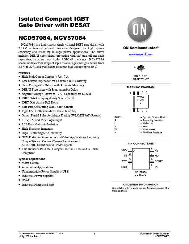
SOIC- 8 NB CASE 751-...


