NCD57200 Overview
Key Specifications
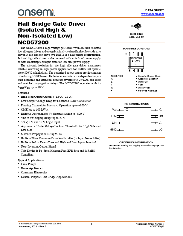
Package: SOP
Operating Voltage: 15 V
Max Voltage (typical range): 20 V
Min Voltage (typical range): 10 V
Key Features
- High Peak Output Current (+1.9 A/- 2.3 A)
- Low Output Voltage Drop for Enhanced IGBT Conduction
- Floating Channel for Bootstrap Operation up to +800 V
- CMTI up to 100 kV/ms
- Reliable Operation for VS Negative Swing to
- VDD & VBS Supply Range up to 20 V
- 3.3 V, 5 V, and 15 V Logic Input
- Asymmetric Under Voltage Lockout Thresholds for High Side and Low Side
- Matched Propagation Delay 90 ns
- Built- in 20 ns Minimum Pulse Width Filter (or Input Noise Filter)