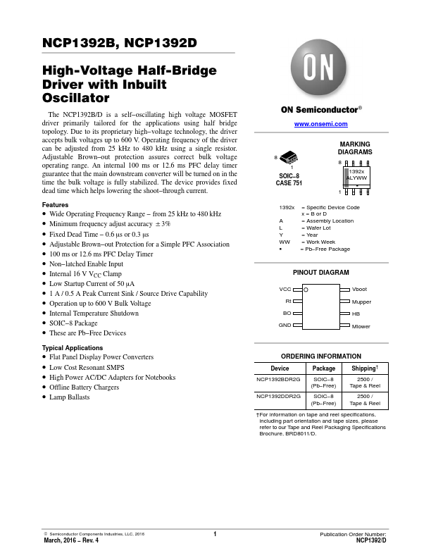
NCP1392D
Overview
- Wide Operating Frequency Range - from 25 kHz to 480 kHz
- Minimum frequency adjust accuracy $3%
- Fixed Dead Time - 0.6 ms or 0.3 ms
- Adjustable Brown-out Protection for a Simple PFC Association
- 100 ms or 12.6 ms PFC Delay Timer
- Non-latched Enable Input
- Internal 16 V VCC Clamp
- Low Startup Current of 50 mA
- 1 A / 0.5 A Peak Current Sink / Source Drive Capability
- Operation up to 600 V Bulk Voltage