NCP167
NCP167 is LDO Regulator manufactured by onsemi.
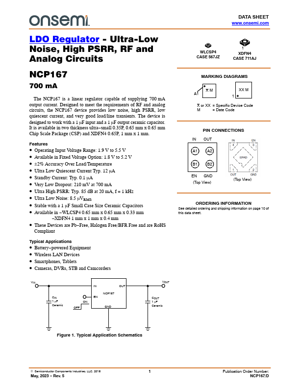
DATA SHEET .onsemi.
LDO Regulator
- Ultra-Low Noise, High PSRR, RF and Analog Circuits
700 mA
The NCP167 is a linear regulator capable of supplying 700 mA output current. Designed to meet the requirements of RF and analog circuits, the NCP167 device provides low noise, high PSRR, low quiescent current, and very good load/line transients. The device is designed to work with a 1 mF input and a 1 mF output ceramic capacitor. It is available in two thickness ultra- small 0.35P, 0.65 mm x 0.65 mm Chip Scale Package (CSP) and XDFN4 0.65P, 1 mm x 1 mm.
Features
- Operating Input Voltage Range: 1.9 V to 5.5 V
- Available in Fixed Voltage Option: 1.8 V to 5.2 V
- ±2% Accuracy Over...