NCP2821
Features http://onsemi. MARKING DIAGRAM
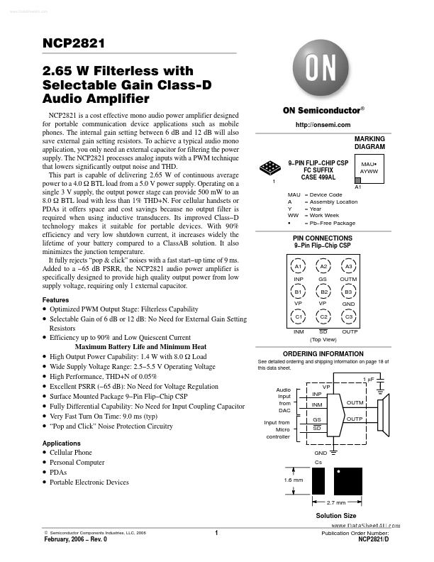
9- PIN FLIP- CHIP CSP FC SUFFIX CASE 499AL MAU A Y WW G MAUG AYWW
A1 = Device Code = Assembly Location = Year = Work Week = Pb- Free Package
PIN CONNECTIONS
9- Pin Flip- Chip CSP
A1 INP B1
A2 GS B2 VP C2
A3 OUTM B3 GND C3
- Optimized PWM Output Stage: Filterless Capability
- Selectable Gain of 6 d B or 12 d B: No Need for External Gain Setting
- Efficiency up to 90% and Low Quiescent Current
- -
- -
- -
- -
- -
- -
Maximum Battery Life and Minimum Heat High Output Power Capability: 1.4 W with 8.0 W Load Wide Supply Voltage Range: 2.5- 5.5 V Operating Voltage High Performance, THD+N of 0.05% Excellent PSRR (- 65 d B): No Need for Voltage Regulation Surface Mounted Package 9- Pin Flip- Chip CSP Fully Differential Capability: No Need for Input Coupling Capacitor Very Fast Turn On Time: 9.0 ms (typ) “Pop and Click” Noise Protection Circuitry Resistors
VP C1 INM
SD OUTP (Top View)
ORDERING INFORMATION
See detailed ordering and shipping information on...