Datasheet Summary
Synchronous PWM Controller
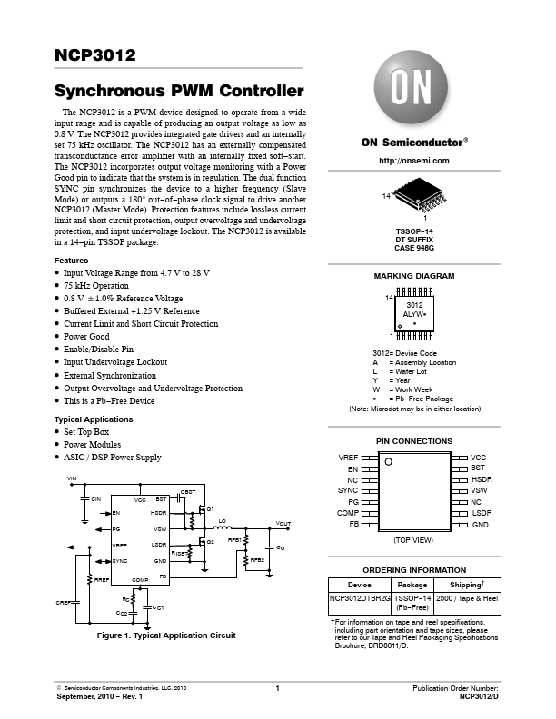
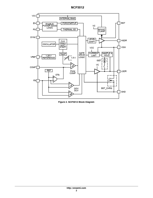
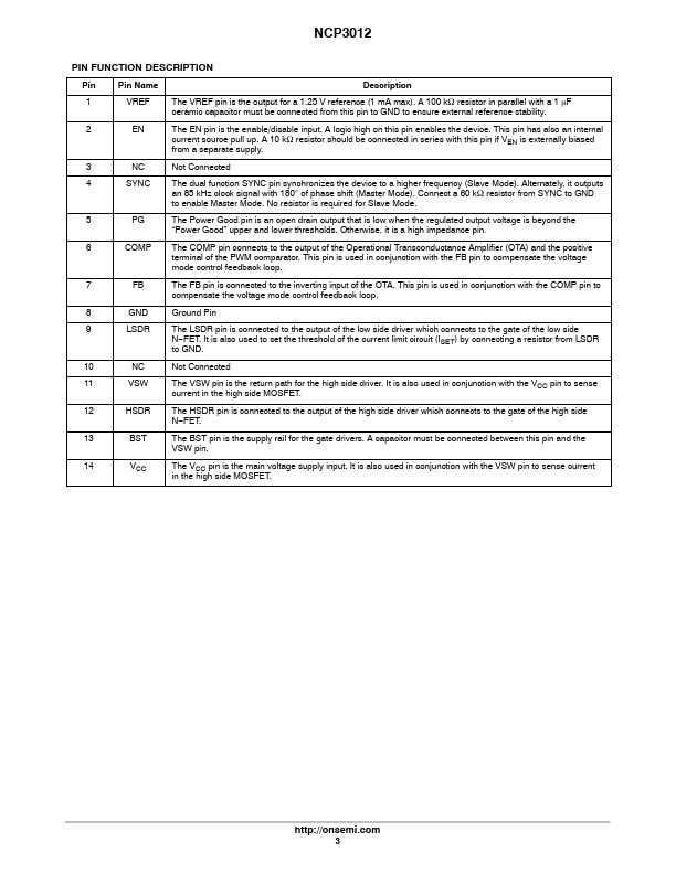
The NCP3012 is a PWM device designed to operate from a wide input range and is capable of producing an output voltage as low as 0.8 V. The NCP3012 provides integrated gate drivers and an internally set 75 kHz oscillator. The NCP3012 has an externally pensated transconductance error amplifier with an internally fixed soft- start. The NCP3012 incorporates output voltage monitoring with a Power Good pin to indicate that the system is in regulation. The dual function SYNC pin synchronizes the device to a higher frequency (Slave Mode) or outputs a 180° out- of- phase clock signal to drive another NCP3012 (Master Mode). Protection Features include lossless...