NCP3030A Overview
Pin Pin Name Description 1 VCC The VCC pin is the main voltage supply input. It is also used in conjunction with the VSW pin to sense current in the high side MOSFET. 2 P The P pin connects to the output of the Operational Transconductance Amplifier (OTA) and the positive terminal of the PWM parator.
NCP3030A Key Features
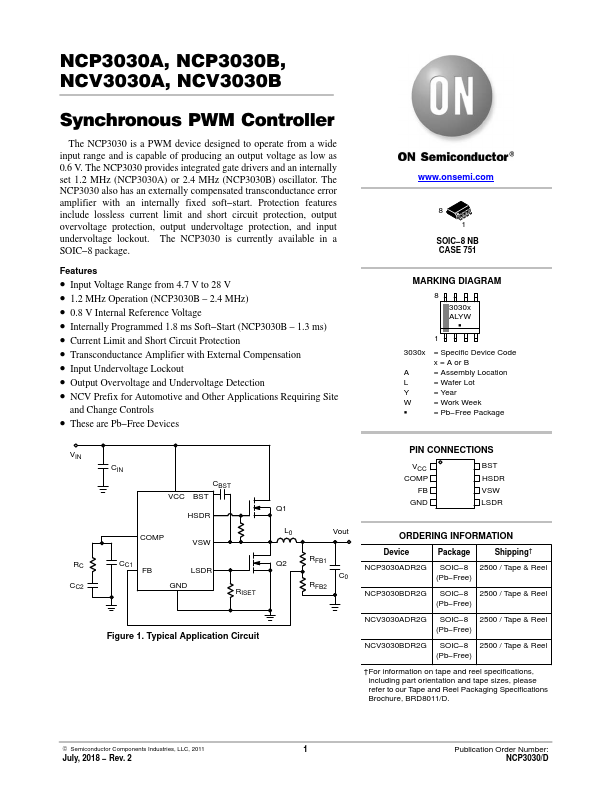
- Input Voltage Range from 4.7 V to 28 V
- 1.2 MHz Operation (NCP3030B
- 2.4 MHz)
- 0.8 V Internal Reference Voltage
- Internally Programmed 1.8 ms Soft-Start (NCP3030B
- 1.3 ms)
- Current Limit and Short Circuit Protection
- Transconductance Amplifier with External pensation
- Input Undervoltage Lockout
- Output Overvoltage and Undervoltage Detection