NCP3125
NCP3125 is 4A Synchronous PWM Switching Converter manufactured by onsemi.
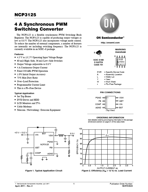
4 A Synchronous PWM Switching Converter
The NCP3125 is a flexible synchronous PWM Switching Buck Regulator. The NCP3125 is capable of producing output voltages as low as 0.8 V. The NCP3125 also incorporates voltage mode control. To reduce the number of external ponents, a number of Features are internally set including switching frequency. The NCP3125 is currently available in an SOIC- 8 package.
Features
- 4.5 V to 13.2 V Operating Input Voltage Range
- 60 m W High- Side, 36 m W Low- Side Switches
- Output Voltage Adjustable to 0.8 V
- 4 A Continuous Output Current
- Fixed 350 k Hz PWM Operation
- 1.0% Initial Output Accuracy
- 75% Max Duty Ratio
- Over- Load Protection
- Programmable Current Limit
- This is a Pb- Free Device
Typical Application
- Set Top Boxes
- DVD Drives and HDD
- LCD Monitors and TVs
- Cable Modems
- Tele / Networking / Data Equipment http://onsemi.
SOIC- 8 NB D SUFFIX CASE 751
MARKING DIAGRAM
8 3125
ALYWXG G
3125 A L Y W
= Specific Device Code = Assembly Location = Wafer Lot = Year/ = Work Week
= Pb- Free Package
PIN CONNECTIONS
PGND FB
P AGND
1 (Top...