Datasheet Summary
4 A Integrated Synchronous Buck Converter
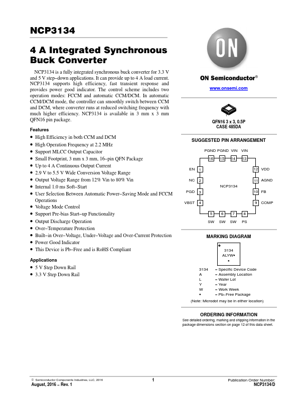
NCP3134 is a fully integrated synchronous buck converter for 3.3 V and 5 V step- down applications. It can provide up to 4 A load current. NCP3134 supports high efficiency, fast transient response and provides power good indicator. The control scheme includes two operation modes: FCCM and automatic CCM/DCM. In automatic CCM/DCM mode, the controller can smoothly switch between CCM and DCM, where converter runs at reduced switching frequency with much higher efficiency. NCP3134 is available in 3 mm x 3 mm QFN16 pin package.
Features
- High Efficiency in both CCM and DCM
- High Operation Frequency at 2.2 MHz
- Support MLCC Output Capacitor
-...