Datasheet4U Logo Datasheet4U.com

NCP451 - 3A Ultra-Small Low Ron and Controlled Load Switch

General Description

Pin Name Pin Number Type IN A2, B2 POWER GND EN OUT C1 C2 A1, B1 POWER INPUT OUTPUT Description Load

switch input voltage; connect a 1 mF or greater ceramic capacitor from IN to GND as close as possible to the IC.

Ground connection.

Enable input, logic high turns on power switch.

Key Features

  • 0.75 V.
  • 5.5 V Operating Range.
  • 12 mW N MOSFET from 3.6 V to 5.5 V.
  • 13 mW N MOSFET from 1 V to 3.3 V.
  • DC Current Up to 3 A.
  • Output Auto.
  • Discharge.
  • Active High EN Pin.
  • WLCSP6 0.9 x 1.4 mm.
  • These Devices are Pb.
  • Free, Halogen Free/BFR Free and are RoHS Compliant Typical.

📥 Download Datasheet

Datasheet Details

Part number NCP451
Manufacturer onsemi
File Size 305.91 KB
Description 3A Ultra-Small Low Ron and Controlled Load Switch
Datasheet download datasheet NCP451 Datasheet

Full PDF Text Transcription (Reference)

The following content is an automatically extracted verbatim text from the original manufacturer datasheet and is provided for reference purposes only.

View original datasheet text
3A Ultra-Small Low Ron and Controlled Load Switch with Auto-Discharge Path NCP451 The NCP451 is a very low Ron MOSFET controlled by external logic pin, allowing optimization of battery life, and portable device autonomy. Indeed, due to a current consumption optimization with NMOS structure, leakage currents are eliminated by isolating connected IC on the battery when not used. Output discharge path is also embedded to eliminate residual voltages on the output rail. 
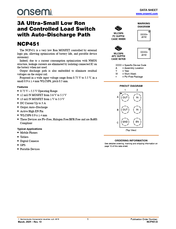
Proposed in a wide input voltage range from 0.75 V to 5.5 V, in a small 0.9 x 1.4 mm WLCSP6, pitch 0.5 mm. Features • 0.75 V – 5.5 V Operating Range • 12 mW N MOSFET from 3.6 V to 5.5 V • 13 mW N MOSFET from 1 V to 3.3 V • DC Current Up to 3 A • Output Auto−Discharge • Active High EN Pin • WLCSP6 0.9 x 1.