NCP502
NCP502 is Voltage Regulator manufactured by onsemi.
NCP502, NCV502
Voltage Regulator
- CMOS Low Iq, Low-Dropout
80 mA
The NCP502 series of fixed output linear regulators are designed for handheld munication equipment and portable battery powered applications which require low quiescent. The NCP502 series Features an ultra- low quiescent current of 40 mA. Each device contains a voltage reference unit, an error amplifier, a PMOS power transistor, resistors for setting output voltage, current limit, and temperature limit protection circuits.
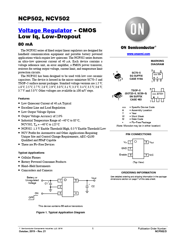
The NCP502 has been designed to be used with low cost ceramic capacitors. The device is housed in the micro- miniature SC70- 5 and TSOP- 5 surface mount packages. Standard voltage versions are 1.5 V, 1.8...